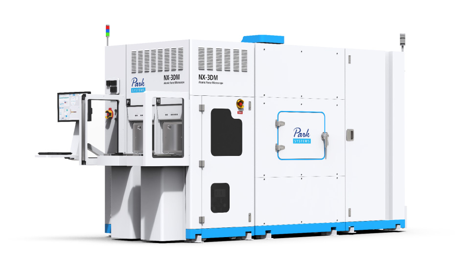
Park NX-3DM is a leading-edge atomic force microscope (AFM) designed for seamless integration into semiconductor fabrication environments. Built on Park Systems’ proven AFM technology, it delivers high-resolution 3D metrology for semiconductor manufacturing while ensuring full compliance with SEMI standards and complete automation. With a strong track record in the semiconductor industry, NX-3DM offers proven reliability and effectiveness for advanced metrology applications.
Key Features
Fully Automated Operation
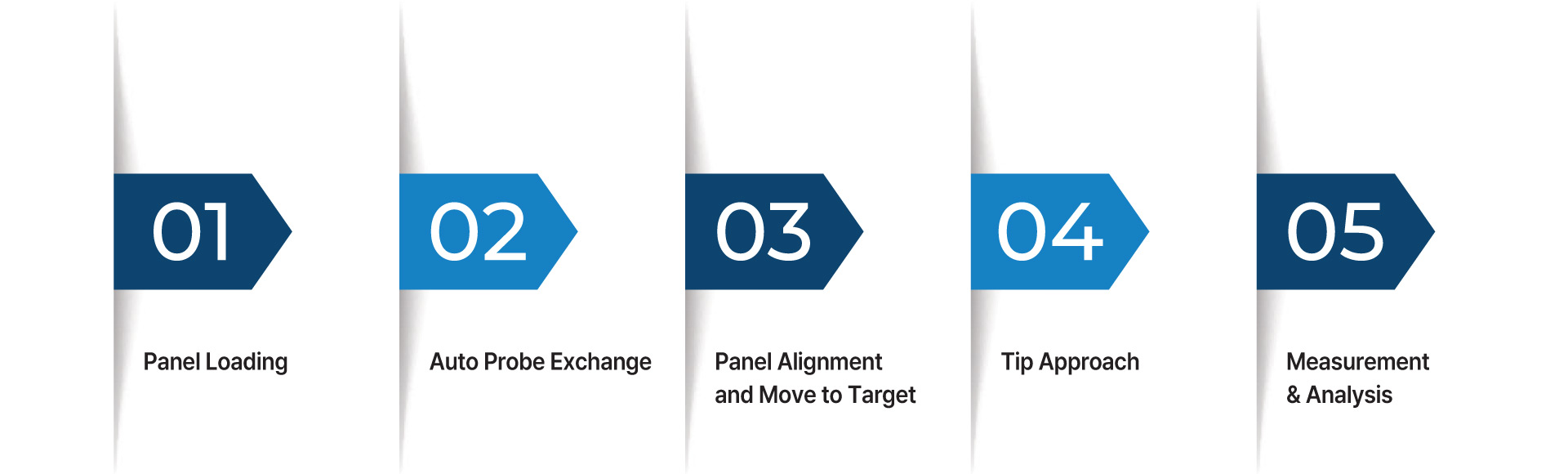
The NX-3DM enables fully automated operation from wafer handling to measurement and analysis. It automatically receives a recipe from a host, performs end-to-end automation by selecting the appropriate tip, scanning multiple target areas, analyzing data, and generating reports.
Innovative Z-Scan System for 3D Measurement
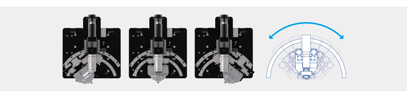
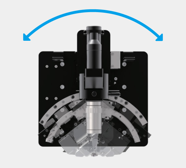
The many unique features of the NX-3DM are made possible by independently tilting the Z-scanner on its patented crosstalk-eliminated platform, where XY and Z scanners are completely decoupled. This design allows users to access vertical sidewalls as well as undercut structures at various angles. Unlike systems with flared tips, this system enables the use of high resolution and high aspect ratio probes.
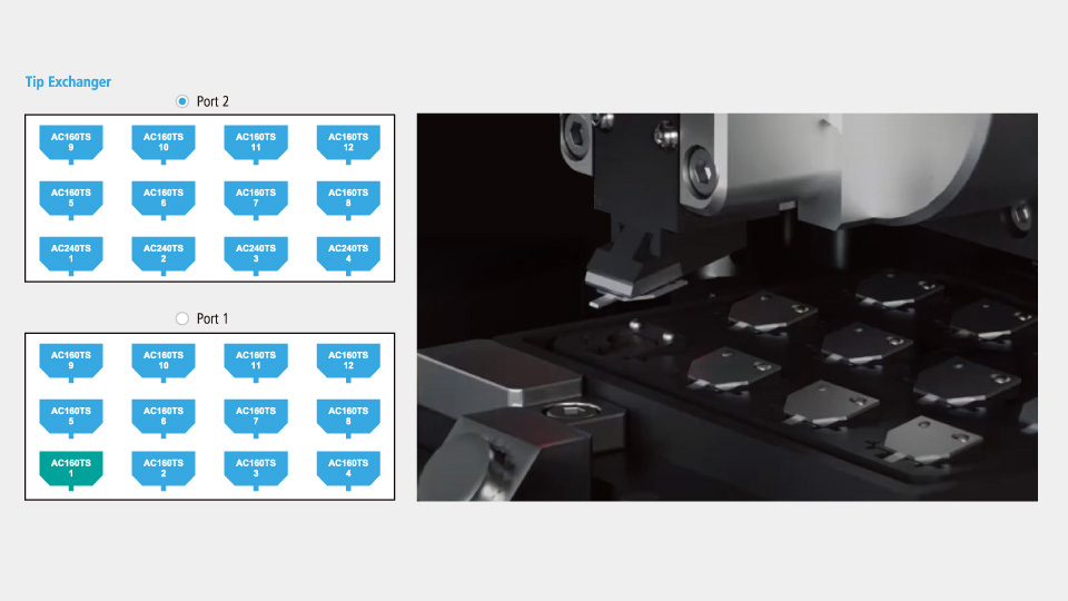
Automatic Probe Exchange
The automatic tip exchanger seamlessly replaces the probe when a threshold is exceeded. It can store up to 24 pre-mounted probes (12 probes per cassette).
Easy-to-Use Operation Software XEA
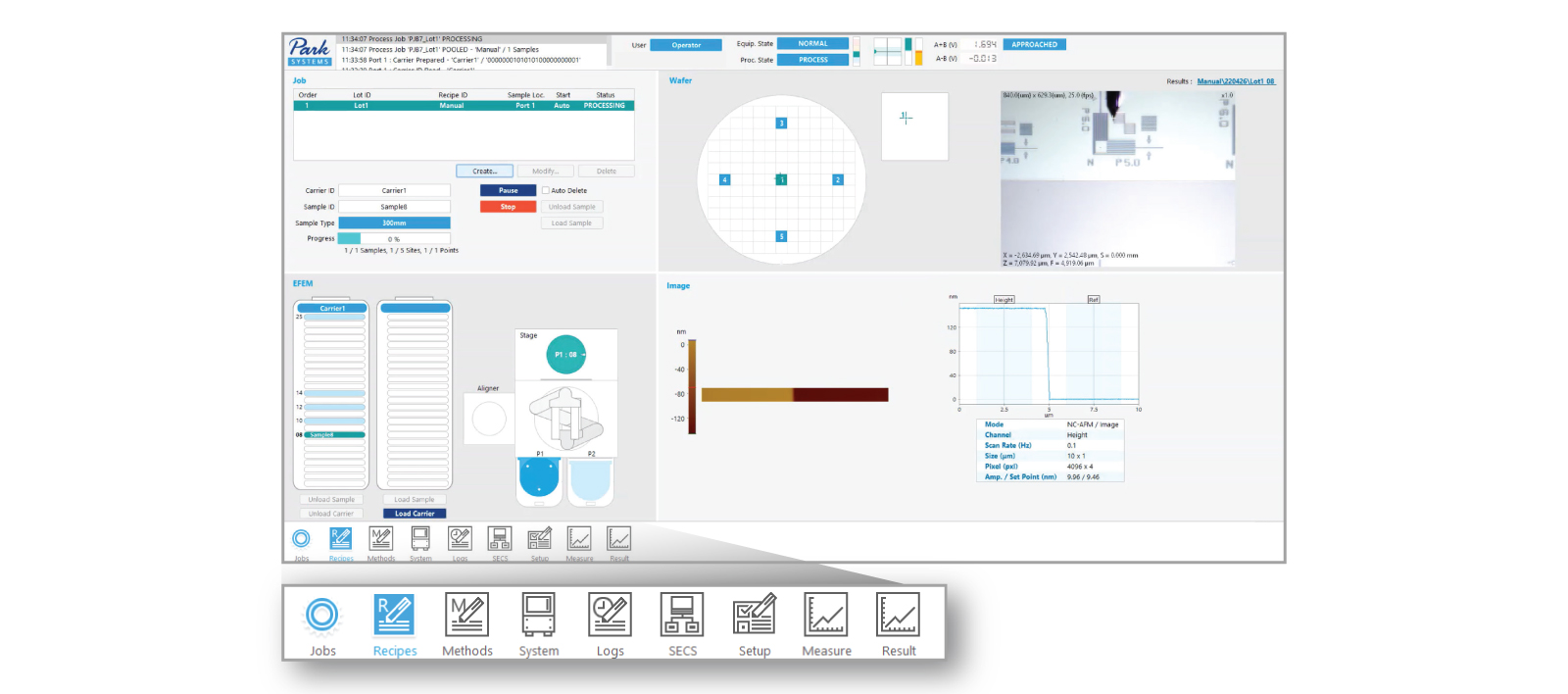
XEA offers practical features such as easy copy/paste of recipes, specialized editing modes, and real-time recipe updates. With built-in functions providing comprehensive system operation—including parameter adjustment, database management, and maintenance—the interface remains straightforward and user-friendly. The navigator provides an intuitive user interface that integrates system adjustment and operation.
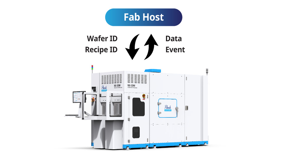
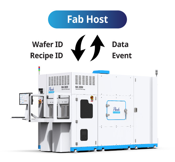
Fab Host Communication via SECS/GEM Protocol
The NX-3DM enables Fab host communication via the SECS/GEM protocol, ensuring full compliance with SEMI standards, including E30, E40, E87, E90, E94, and E84 PI/O for AMHS integration.
Fab Compatibility According to SEMI Standards
The NX-3DM ensures optimal compatibility with cleanroom environments in semiconductor fabs. The system achieves ISO Cleanliness Class 1 (≤10 particles/m³ ≥ 0.1 µm and ≤2 particles/m³ ≥ 0.2 µm) and minimizes particle contamination along the wafer movement path through its engineered fan filter unit and ventilation system, while maintaining efficient noise shielding. Additional chemical filters are available as options to effectively block airborne molecular contamination (AMC), which can adversely affect sensitive samples. Furthermore, the system is equipped with advanced monitoring capabilities that can detect and alert users to potential fire hazards or voltage sags.
Park AFM Technology
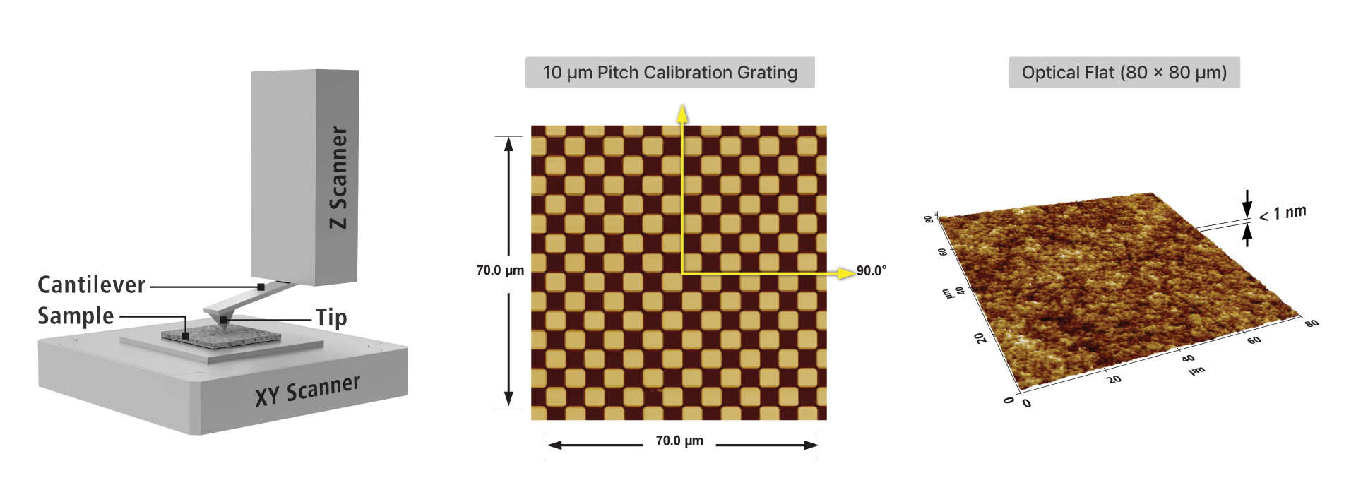
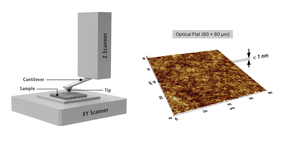
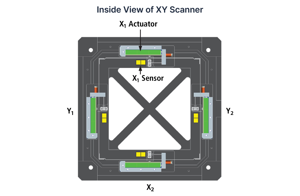
Orthogonal Scan System
The separated flexure-guided 2D XY scanner and 1D Z scanner system minimizes out-of-plane motion by eliminating crosstalk between horizontal and vertical motion. The independent Z scanner enables precise, linear, and fast dynamic performance.
The XY scanner features a dual-servo architecture with two pairs of actuators and position sensors mounted on opposite sides of each axis, providing
precise orthogonality and accurate positioning across the entire scan area.
Park AFM Technology
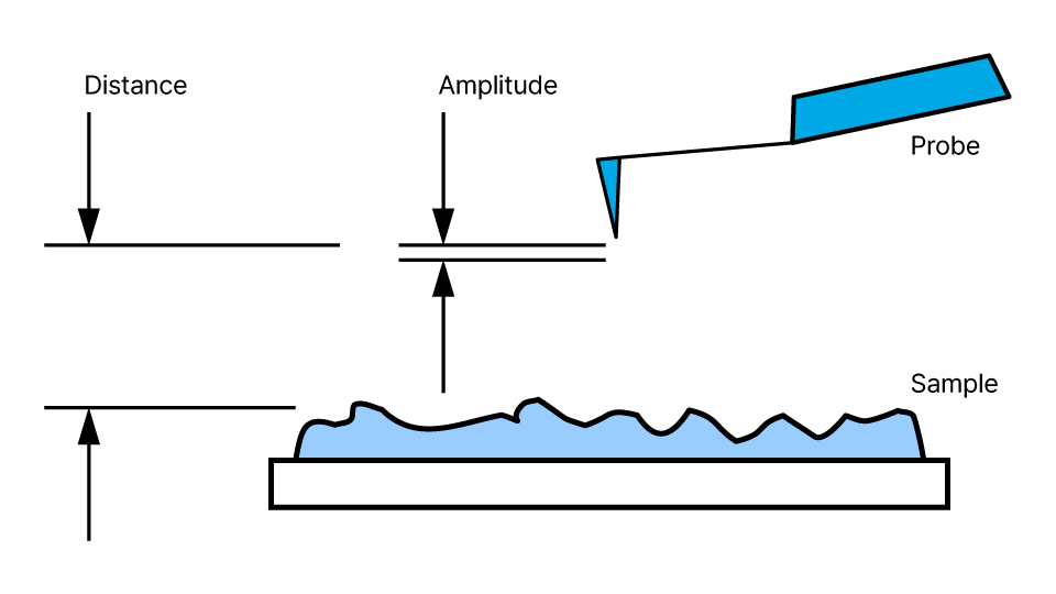
True Non-Contact™ Mode
True Non-contact™ mode, a proprietary technology offered by Park Systems, obtains topography by detecting the attractive van der Waals force between the tip and sample surface. The key advantage of True Non-contact mode is the prevention of tip wear and sample damage, ensuring consistent results with superior data reliability. This also reduces the total cost of ownership by extending tip life.
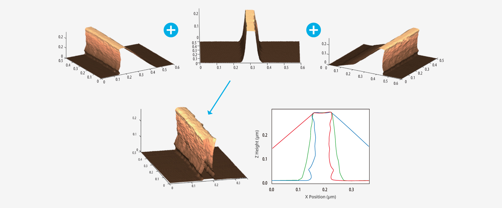
The NX-3DM provides unique access to undercut and overhang structures in photoresist and other industrial materials, ensuring users receive accurate topographical data across the entire sample. Images taken at three different tilting angles can be automatically stitched together to form a complete 3D image.
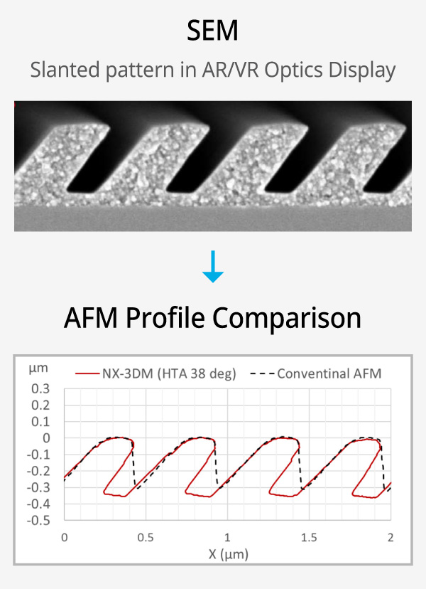
AR/VR Optics Display Structure
The NX-3DM tilts the AFM head to capture true 3D sidewall topography, enabling non-destructive, precise measurement of steep and even highly undercut angles.
Conventional SEM/TEM cross-sectioning is destructive, while conventional AFM is limited by tip geometry, making it difficult to accurately measure steep or highly undercut sidewalls.
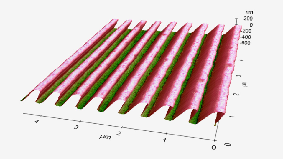
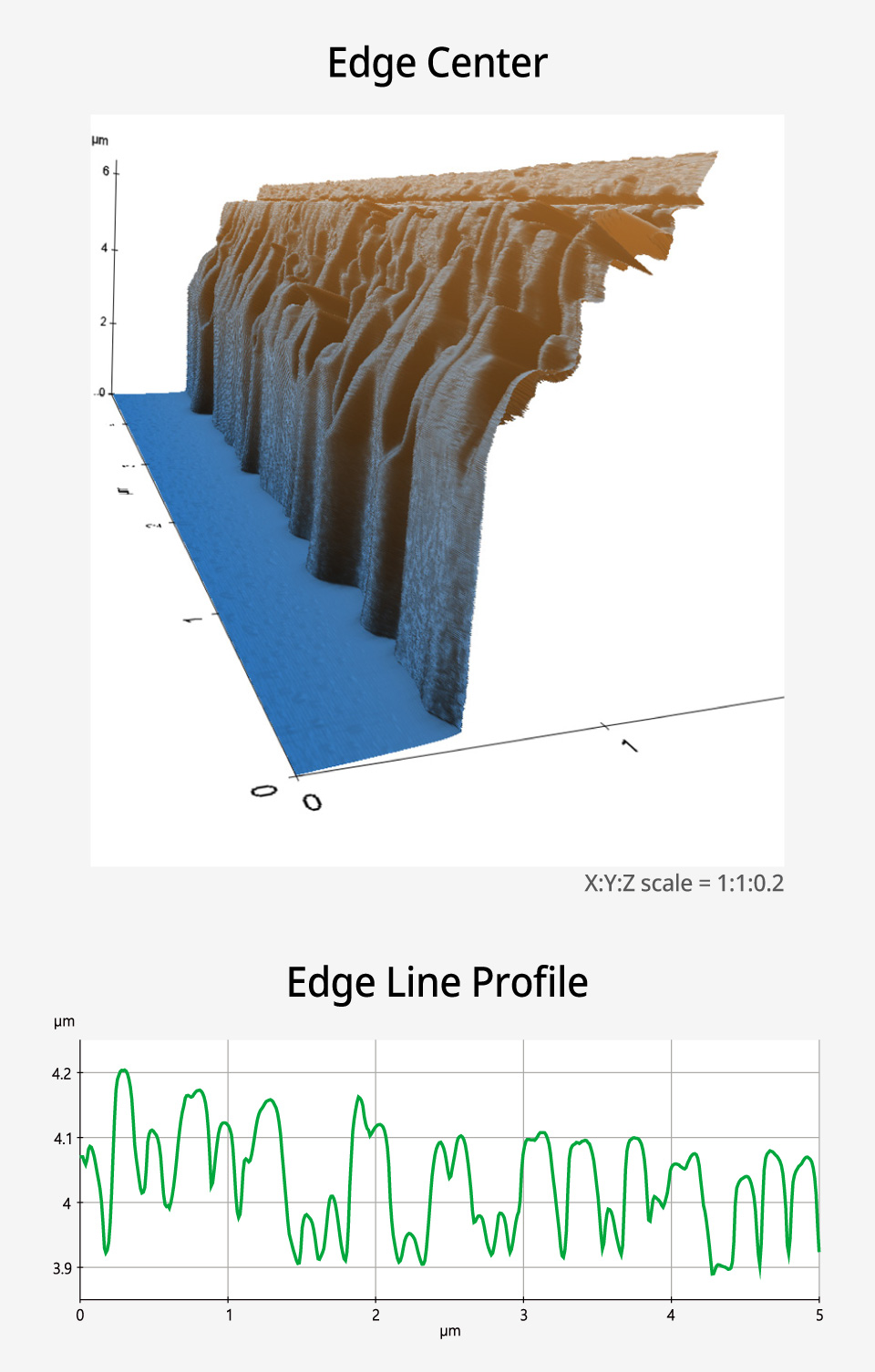
Sidewall Roughness Measurement
The NX-3DM’s innovative head-tilting design provides access to sidewalls with an ultra-sharp tip, enabling high-resolution, well-defined measurement of sidewall roughness. This allows precise characterization of sidewall topography, including fine surface variations and irregularities critical to process control and device performance in semiconductor manufacturing.
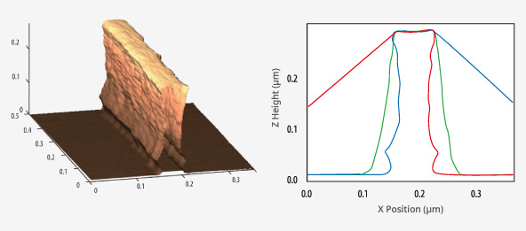
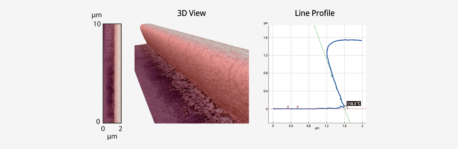
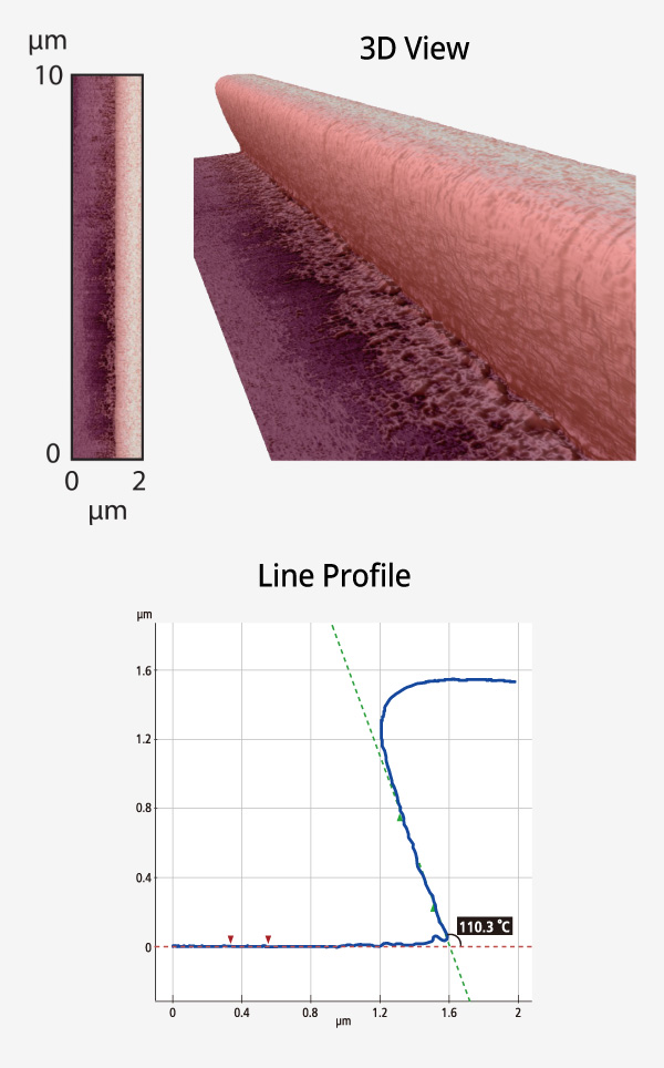
Photoresist Sidewall Angle and Undercut Measurement
The NX-3DM’s True Non-contact™ mode enables precise measurement of sidewall angle in photoresist patterns without causing sample deformation, and accurately resolving undercut profiles critical to lithography process control. As demonstrated in the line profile, NX-3DM captures the full sidewall geometry at an isotropic scale, revealing a sidewall angle of 110.3°