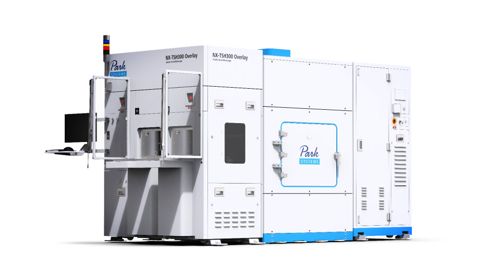
Park NX-TSH300 Overlay overcomes the limitations of traditional sample-scanning AFM systems. Designed specifically for measuring heavy, large, and high-bow 300 mm wafers, it employs a revolutionary Tip Scanning Head (TSH) technology combined with an anti-warpage sample chuck. By moving the scanner instead of the sample, it ensures high-speed, high-precision metrology regardless of wafer weight or warpage. Integrated with high-resolution vision and optional optical modules, it maximizes overlay alignment accuracy and yield for advanced semiconductor packaging.
Key Features
Fully Automated Operation
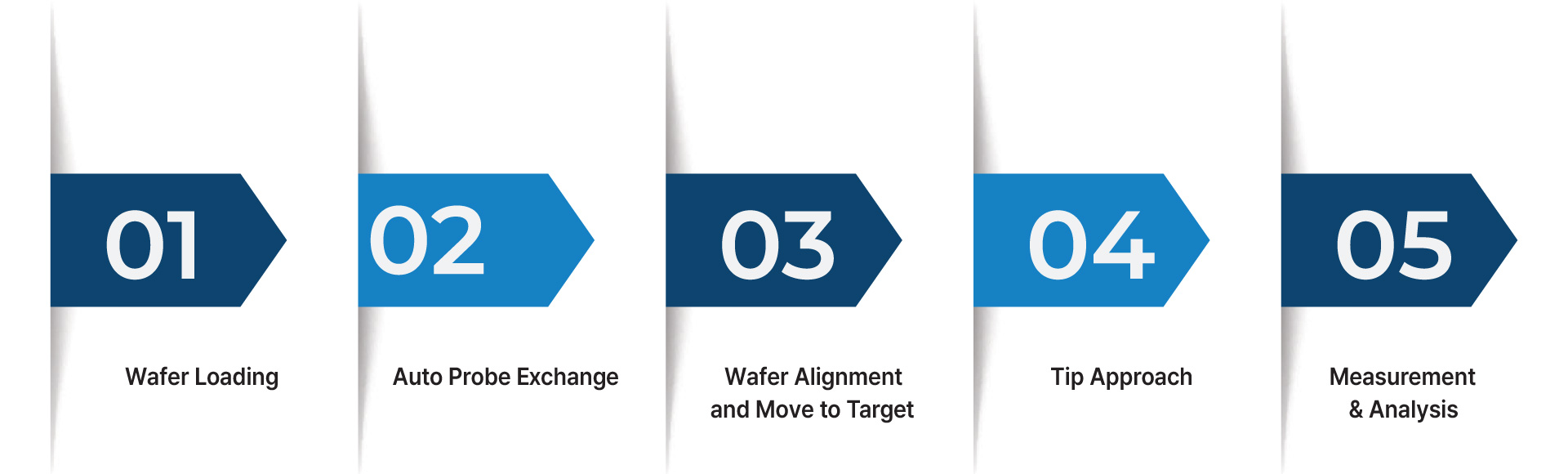
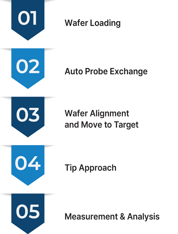
NX-TSH300 Overlay enables fully automated operation for high-volume manufacturing (HVM) environments, covering the entire workflow from wafer handling to measurement and analysis. It automatically receives a recipe from a host and executes the full sequence—selecting the appropriate tip, scanning multiple target areas, analyzing data, and generating reports.
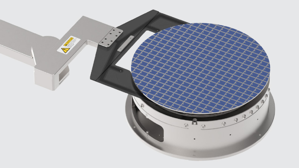
Automated Wafer Handling Capability
Wafer transfer is performed automatically by an equipment front end module (EFEM). It uses robotic mechanisms, sensors, and algorithms to ensure precise alignment and reliable handling of various materials, including warped wafers.
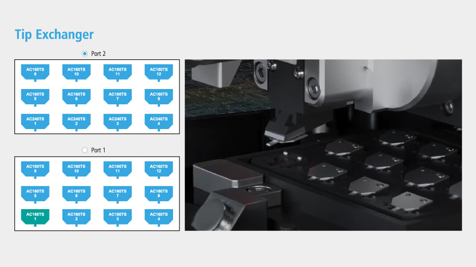
Automatic Probe Exchange
The automatic tip exchanger seamlessly replaces the probe when a threshold is exceeded. It can store up to 24 pre-mounted probes (12 probes per cassette).
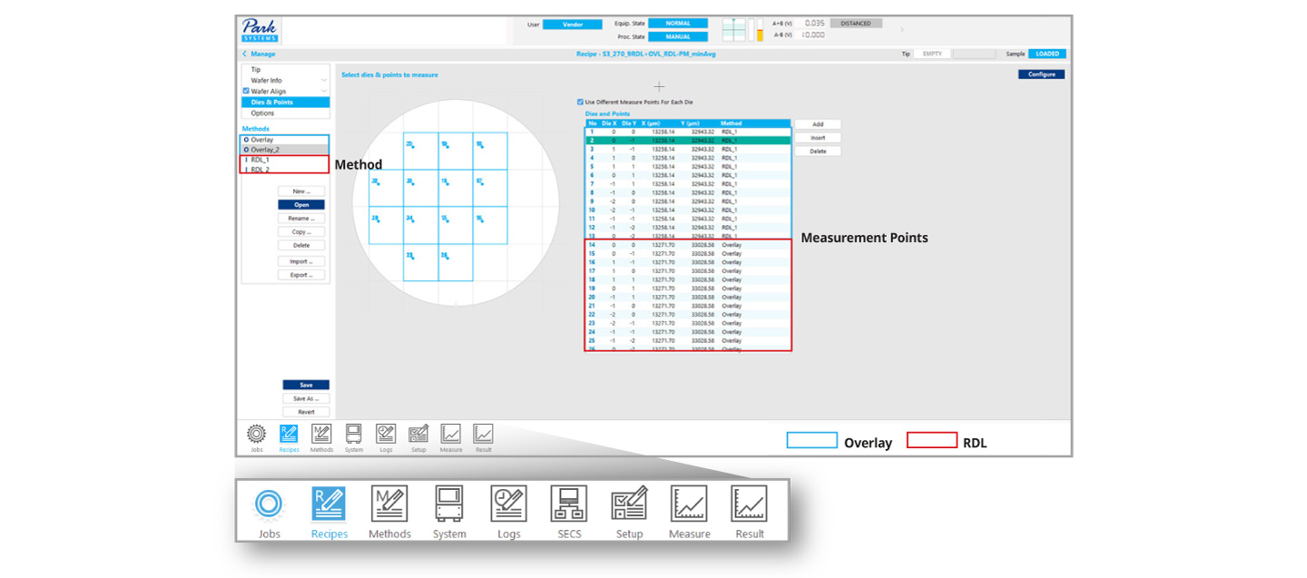
Single Recipe for Both Overlay and RDL
XEA offers practical features such as easy copy/paste of recipes, specialized editing modes, and real-time recipe updates. Additionally, a single recipe supports both overlay and RDL measurement methods. With built-in functions providing comprehensive system operation—including parameter adjustment, database management, and maintenance—the interface remains straightforward and user-friendly. The navigator provides an intuitive user interface that integrates system adjustment and operation.
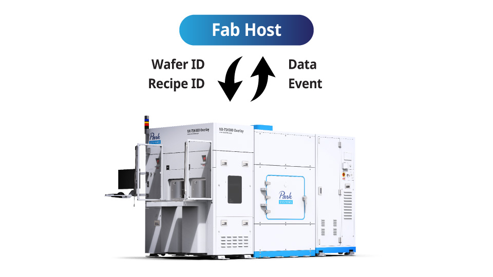
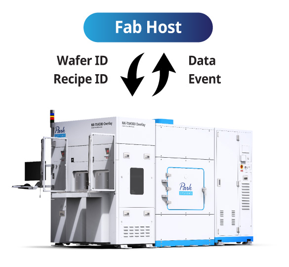
Fab Host Communication via SECS/GEM Protocol
The system enables Fab host communication via the SECS/GEM protocol, ensuring full compliance with SEMI standards, including E30, E40, E87, E90, E94, and E84 PI/O for AMHS integration.
Fab Compatibility According to SEMI Standards
NX-TSH300 Overlay ensures optimal compatibility with cleanroom environments in semiconductor fabs. The system achieves ISO Cleanliness Class 1 (≤10 particles/m³ ≥ 0.1 µm and ≤2 particles/m³ ≥ 0.2 µm) and minimizes particle contamination along the tape frame movement path through its engineered fan filter unit and ventilation system, while maintaining efficient noise shielding. Furthermore, the system is equipped with advanced monitoring capabilities that can detect and alert users to potential fire hazards or voltage sags.
Park AFM Technology
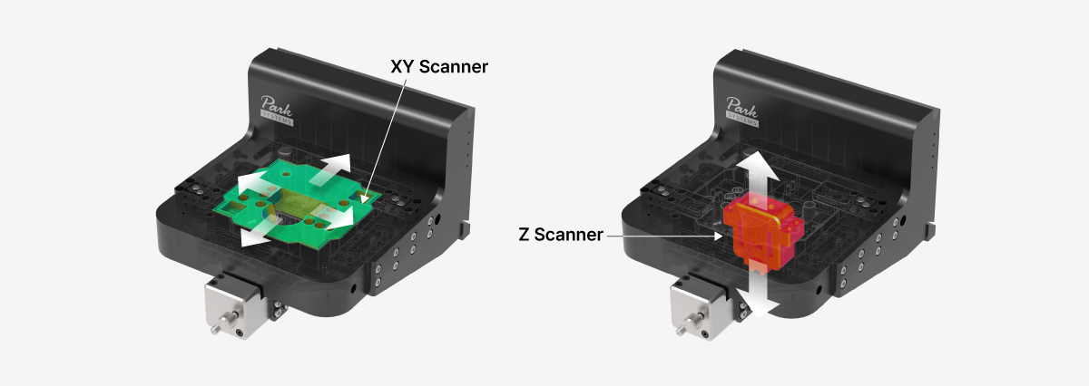
Tip Scanning Head (TSH) System
The sample is secured on the chuck while the gantry-mounted tip scanning head moves to desired measurement positions on the sample surface. This tip scanning approach eliminates sample size and weight limitations. The tip scanning head features fully decoupled XY and Z scanners,enabling precise control in each direction.
Decoupled XY and Z Scanner System
The separate flexure-guided 2D XY scanner and 1D Z scanner system minimizes out-of-plane motion by eliminating crosstalk between horizontal and vertical motion. The independent Z scanner enables precise, linear, and fast dynamic performance.
Park AFM Technology
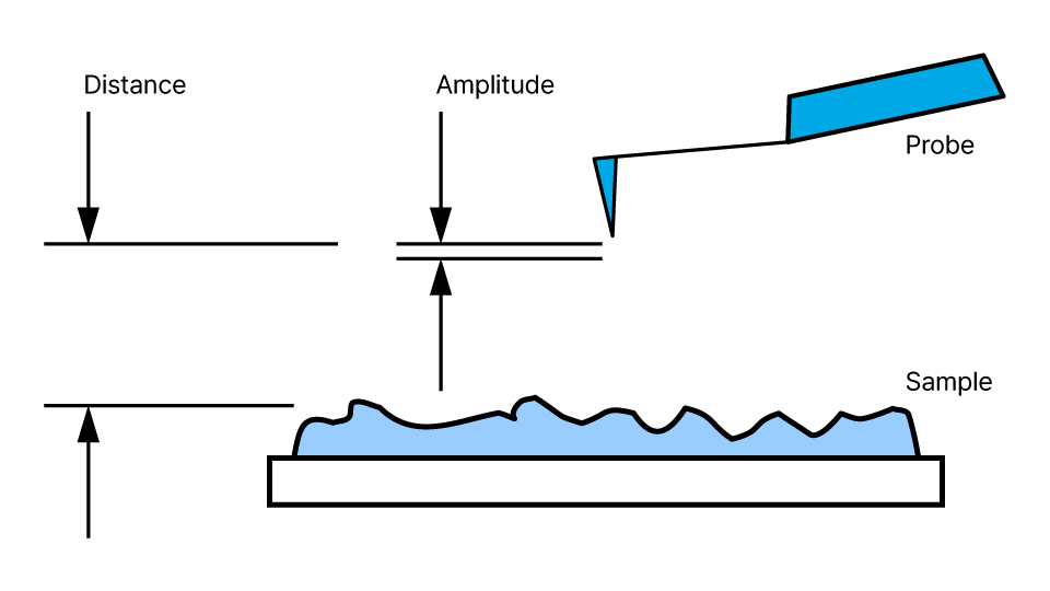
True Non-Contact™ Mode
True Non-contact™ mode, a proprietary technology offered by Park Systems, obtains topography by detecting the attractive van der Waals force between the tip and sample surface. The key advantage of True Non-contact mode is the prevention of tip wear and sample damage, ensuring consistent results with superior data reliability. This also reduces the total cost of ownership by extending tip life.
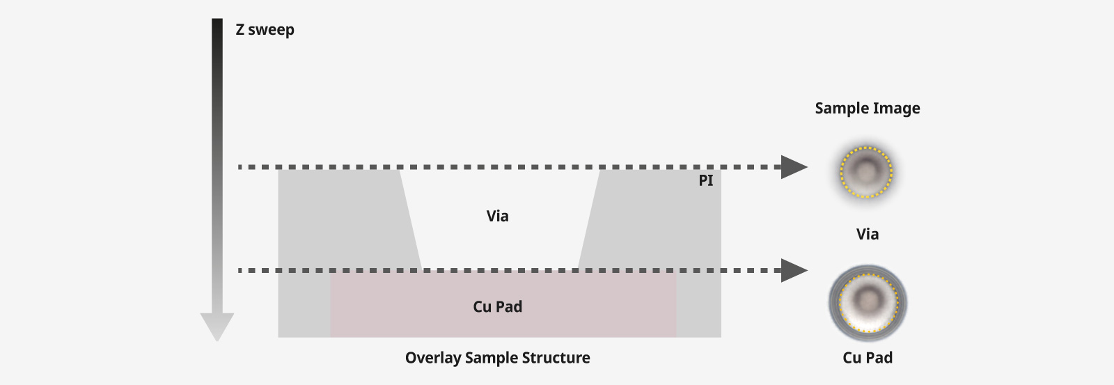
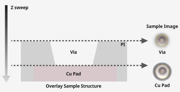
Park Systems' well-established AFM Z scanner technology forms the foundation for an independent Z scanner, offering a 30 µm sweeping range with AFM-level precision to find the optimal focal plane. A high-resolution (HR) and shallow Depth of Focus (DOF) objective lens enhances image contrast and facilitates profile edge detection. By comparing the concentric circles of each layer obtained in this way, the offset value can be automatically measured.
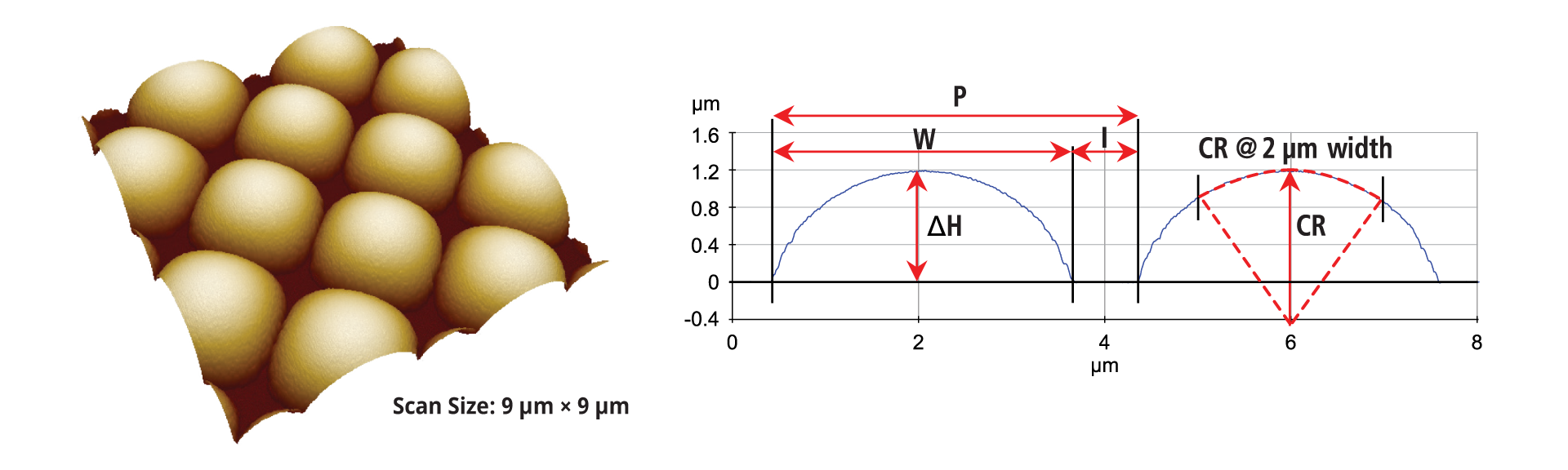
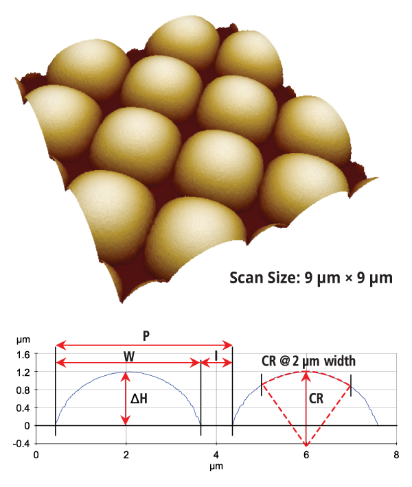
Comprehensive 3D Nano-Metrology
Park AFM accurately measures challenging patterns such as micro-lenses that are difficult to characterize with optical metrology tools, while providing comprehensive analytical capabilities including measurements of width, interval, pitch, height, and radius of curvature.
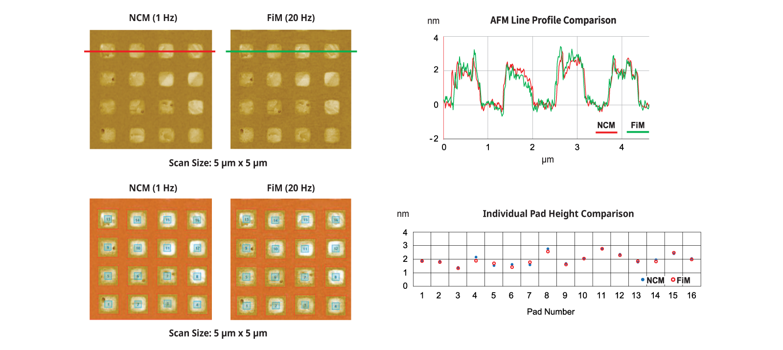
High-Throughput Measurement for Cu Pad
Park’s fast imaging mode (FiM) provides reliable data for Cu pad measurements with high throughput. The Cu pad data from the fast imaging mode delivers line profiles and height values equivalent to those obtained in True Non-contact™ mode. The proprietary analysis algorithm can analyze each Cu pad regardless of pad shape or array arrangement.
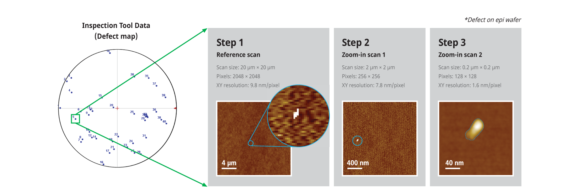
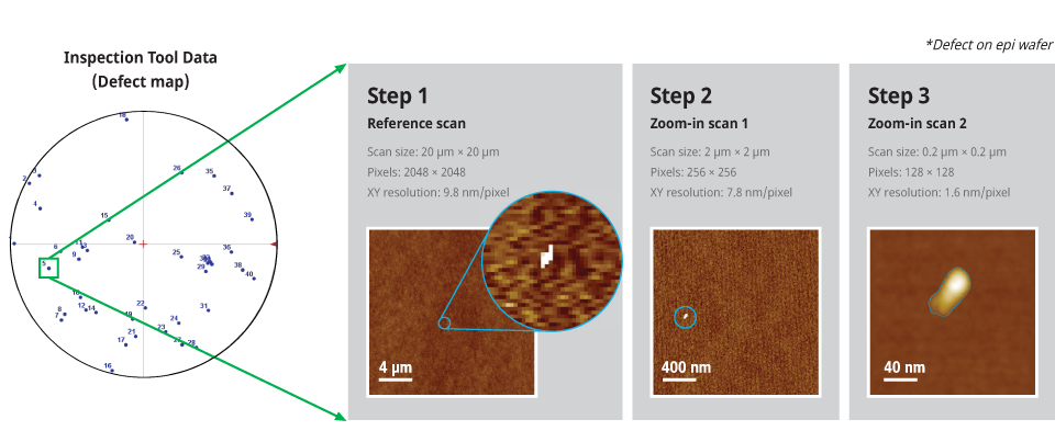
Automatic Defect Review (ADR)
The ADR function provides further analysis of defects detected by conventional defect inspection tools. The defects are automatically scanned by AFM once inspection tool data with defect coordinates is uploaded. Defect types and profiles are automatically analyzed in detail using zoom-in scan data.