Imaging Spectroscopic Ellipsometry (ISE) is an all-optical, non-contact metrology technique that excels at the layer-thickness and material characterization of micro-structured thin-film samples and substrates. The technique combines the benefits of ellipsometry and optical microscopy in a single device and offers enhanced spatial resolution expanding ellipsometry into new areas of microanalysis, microelectronics, and bio analytics.
In this webinar series, we show the benefits of ISE in the field of 2D materials characterization, in which it enables the determination of optical properties. This data is required for a better understanding of 2D material based devices.
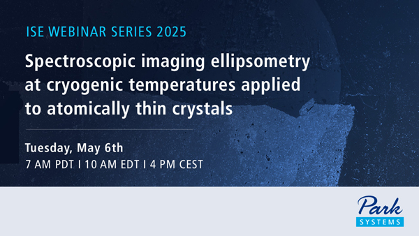
Tuesday, May 6th
Spectroscopic Imaging Ellipsometry at Cryogenic Temperatures Applied to Atomically Thin Crystals
7 AM PDT I 10 AM EDT I 4 PM CEST
Speaker: Prof. Dr. Ursula Wurstbauer,
University of Münster, Germany
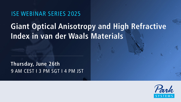
Thursday, June 26th
Giant Optical Anisotropy and High Refractive Index in van der Waals Materials
9 AM CEST I 3 PM SGT I 4 PM JST
Speaker: Georgy Ermolaev, XPANCEO, United Arab Emirates
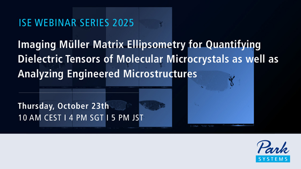
Thursday, October 23th
Imaging Müller Matrix Ellipsometry for Quantifying Dielectric Tensors of Molecular Microcrystals as well as Analyzing Engineered Microstructures
10 AM CEST I 4 PM SGT I 5 PM JST
Speaker: Prof. Dr. Manuela Schiek,
University of Linz, Austria
Thursday, November 20th
Deeper insights into 2D-Materials and related Microcrystals by Imaging Spectroscopic Ellipsometry (ISE) and Imaging Mueller Matrix Ellipsometry (IMME)
7 AM CEST I 3 PM SGT I 4 PM JST
Speaker: Dr. Peter H. Thiesen,
Park Systems GmbH, Accurion Division
Application Note
Investigation of optical and electronic properties of trapped bubbles in vdW heterostructures based on combined ISE and AFM techniques
Application Note
Full Scale Wafer Analysis by Imaging Ellipsometry and Ellipsometric Contrast Micrography (ECM)