SPEAKERS
-
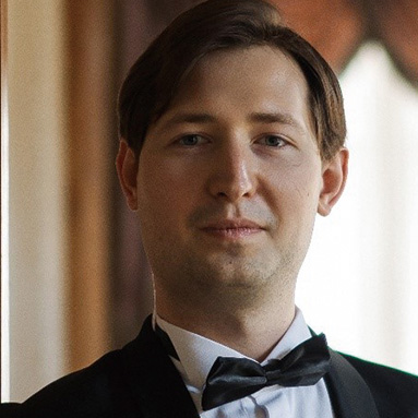
Georgy Ermolaev
Emerging Technologies Research Center, XPANCEO, Dubai00000, United Arab Emirates
Georgy Ermolaev received a Ph.D. in “Broadband optical properties of MoS2 for photonic applications” in 2022 from the Moscow Institute of Physics and Technology. After receiving a Ph.D. Georgy Ermolaev became Research Studies Manager in Xpanceo (Dubai, United Arab Emirates), a deep tech company specializing in next-generation optoelectronic devices. In 2023 Georgy Ermolaev also joined the University of Rome Tor Vergata (Rome, Italy) as a Visiting Researcher. His research interest encompasses various areas, such as ellipsometry, 2D and quantum materials, integrated nanophotonics, biosensors, plasmonics, scanning near-field optical microscopy, and smart contact lenses. Georgy Ermolaev has an impressive publication record, with over 50 published papers and more than 1500 citations during the last 5 years.
- Access Speaker Publications
SPEAKERS
-

- Georgy Ermolaev
- Emerging Technologies Research Center, XPANCEO, Dubai00000, United Arab Emirates
Authors
Related Contents
Advanced Methods for Research into Ferroelectric Materials and Superlattices
Deeper insights into 2D-Materials and related Microcrystals by Imaging Spectroscopic Ellipsometry (ISE) and Imaging Mueller Matrix Ellipsometry (IMME)
