
Si/SiO₂ Patterns
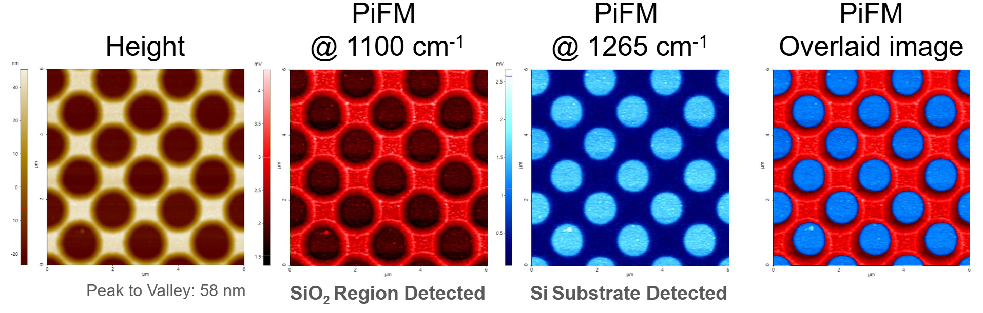
SiO2 patterns formed on a Si substrate provide well-defined chemical and topographic contrast, serving as a model structure for material-specific infrared characterization.
PiFM imaging at selected wavenumbers (1,100 and 1,265 cm⁻¹) distinctly differentiates SiO2 and Si regions by their IR responses, and the overlaid image intuitively visualizes the material distribution together with the surface topography.
Scanning Conditions
-System: FX200 IR
-Scan Rate: 0.5 Hz
-Scan Mode: PiFM
-Pixels: 256 × 56
-Scan Size: 6 µm × 6 µm
-Cantilever: PPP-NCHPt (k=42 N/m, f=330 kHz)
Related Contents
.jpeg)

×