
Patterned Wafer
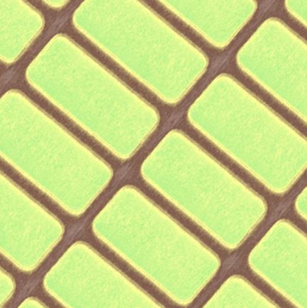
The patterned wafer was characterized using Heterodyne KPFM in potential mode. The scan image clearly reveals the patterned structures with a peak-to-valley potential difference of about 681 mV.
Scanning Conditions
- System: NX15
- Scan Mode: Heterodyne KPFM (Channel: KPFM Potential)
- Scan Rate: 0.3 Hz
- Scan Size: 14 µm × 14 µm
- Pixel Size: 512 × 256 pixels
- Peak-to-valley: 681 mV
Related Contents


×