
Ge atom layer etching (ALE) on Patterned Wafer
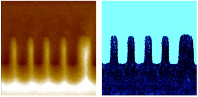
The cross section of a Ge atom layer etching (ALE) patterned wafer was characterized using Scanning Spreading Resistance Microscopy (SSRM). The measurement clearly resolved the trench patterns, showing a peak-to-valley height (left) of 3.4 nm and a corresponding resistance (right) of 73 GΩ.
Scanning Conditions
- System: NX20
- Sample: Germanium atom layer etching(ALE) on Patterned Wafer
- Scan Mode: Scanning spread resistance microscopy (Channel: Height, Resistance)
- Scan Rate: 1 Hz
- Scan Size: 0.5 µm × 0.5 µm
- Pixel Size: 118 nA, 73 GΩ
Related Contents


×