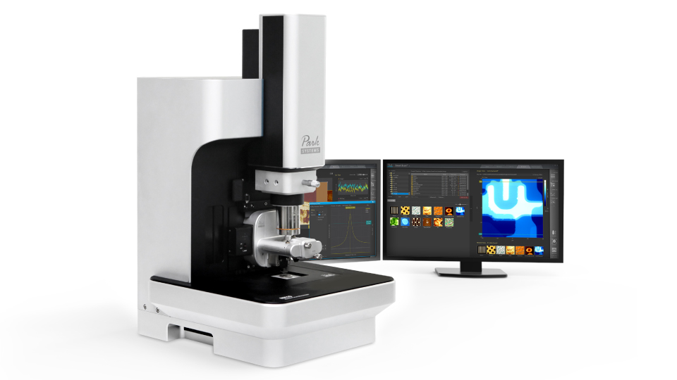
Park NX10 is a flagship atomic force microscope (AFM) designed for small-sample research, delivering unmatched accuracy, reliability, and ease of use. As Park Systems’ original small-sample AFM, it has earned global recognition in both academic and industrial laboratories for producing precise, repeatable nanoscale measurements.
At the core of the NX10 are Park’s proprietary orthogonal scan system and True Non-contact™ mode, innovations that virtually eliminate lateral motion artifacts while protecting both tip and sample. Together, these technologies ensure artifact-free, high-resolution imaging even for the most delicate or challenging samples.
From materials science to polymers and bioengineering, NX10 delivers robust performance and dependable results, making it a trusted platform for advanced nanoscale metrology.
Key Features
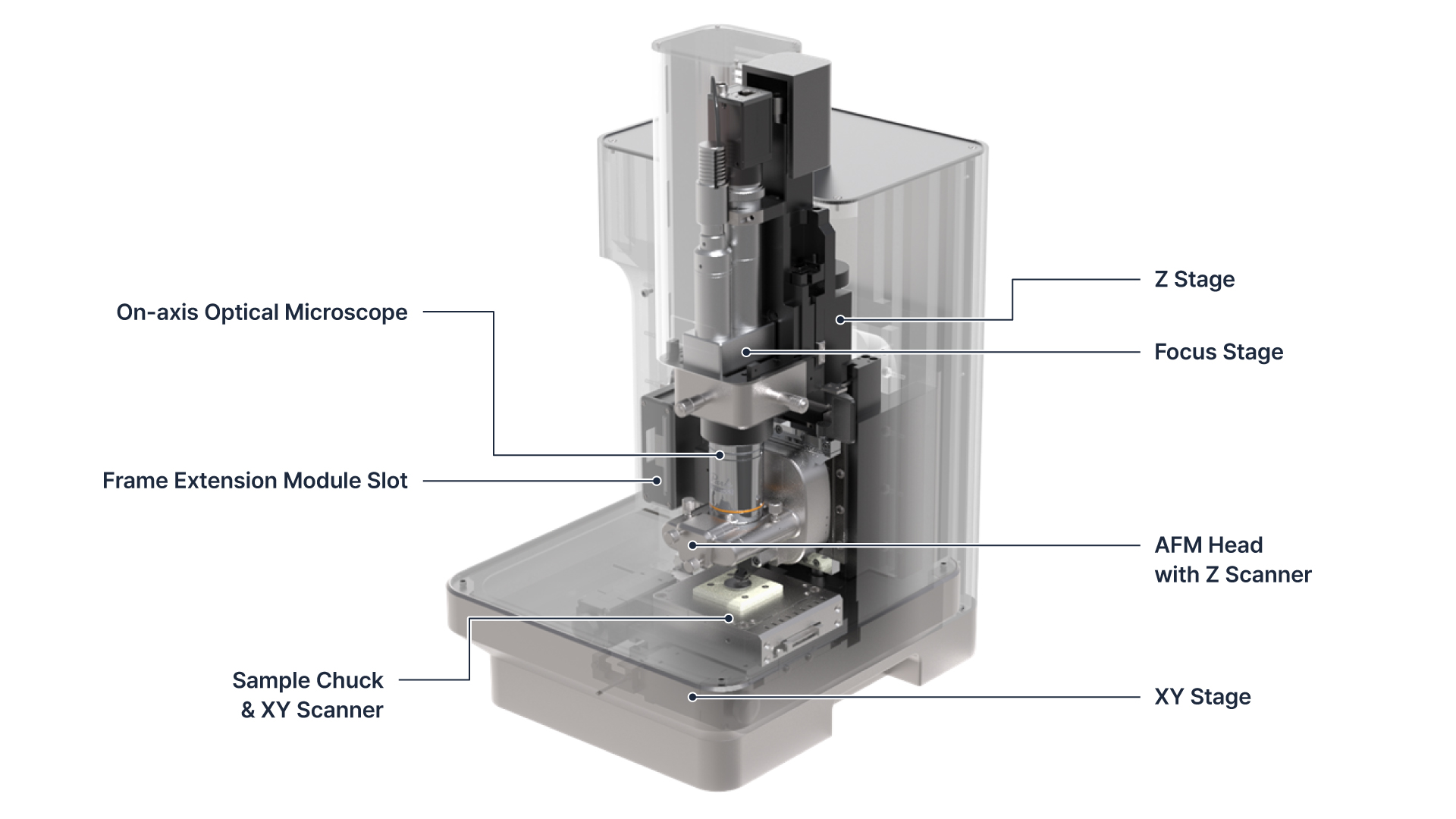
Outstanding NX Mechanical Design
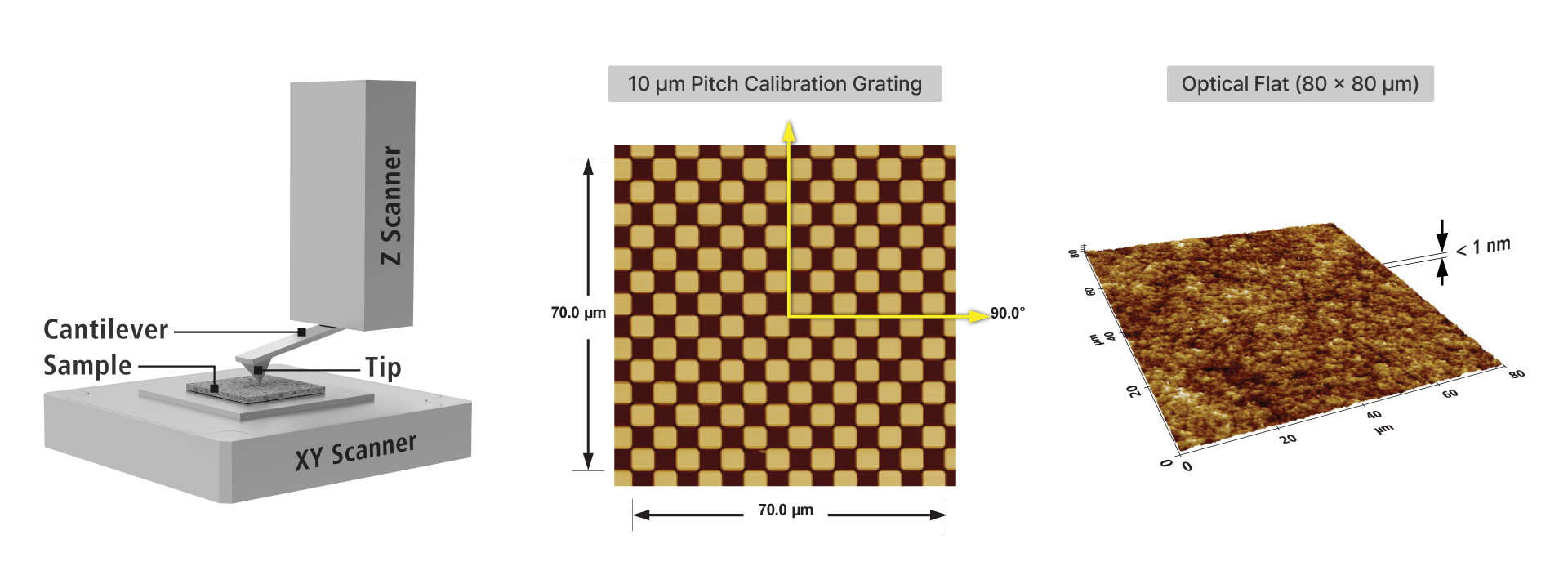
NX10 is built around improved XY and Z scanner performance. This includes fast Z-servo speed, which gives quick vertical response, and improved Z scan straightness for accurate imaging. In addition, the XY scanner ensures precise positioning during scans.
Another highlight is the low Z detector noise. Thanks to the stacked piezo actuator and strain gauge sensor, the NX provides both high precision and exceptionally low noise levels, which are critical for reliable measurements. Together, these features make the NX series a robust and precise platform for advanced AFM research.
Fast Z Servo and High Resolution
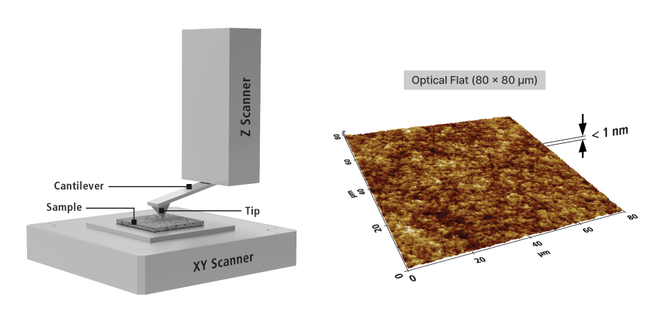
The resolution of the images in Park NX series has been further enhanced. The NX Z scanner, built with a stacked piezo actuator and a strain gauge sensor, delivers fast and precise measurements across a wide range of surfaces. From extremely flat to rough samples, it maintains consistent roughness linearity regardless of scan size, ensuring reliable results in any measurement.
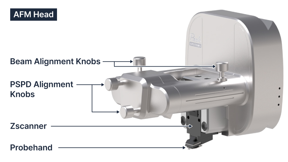
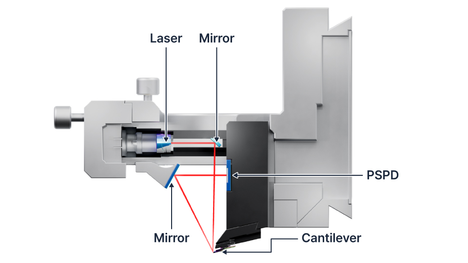
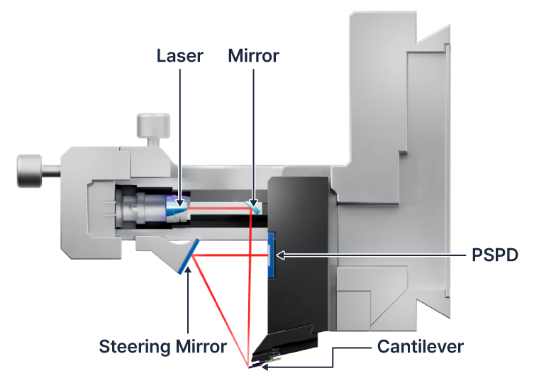
NX Laser Beam Path
The NX head integrates a superluminescent diode that provides low coherence illumination, minimizing interference for stable signal detection. The laser beam is guided through precision mirrors to the cantilever and position-sensitive photodetector (PSPD), ensuring accurate signal alignment.
The knobs move the laser beam directly along the X and Y axes, allowing intuitive adjustment of the beam position and effortless realignment during probe replacement.
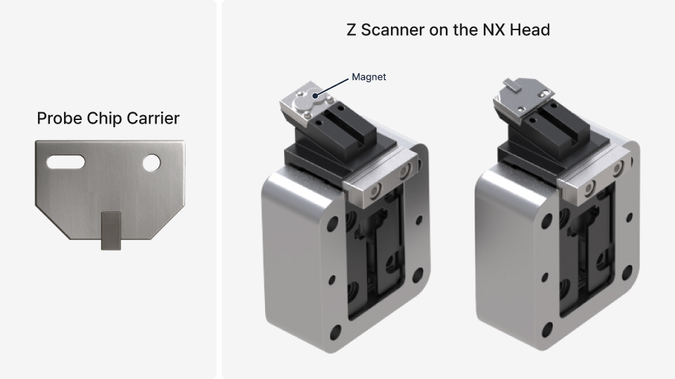
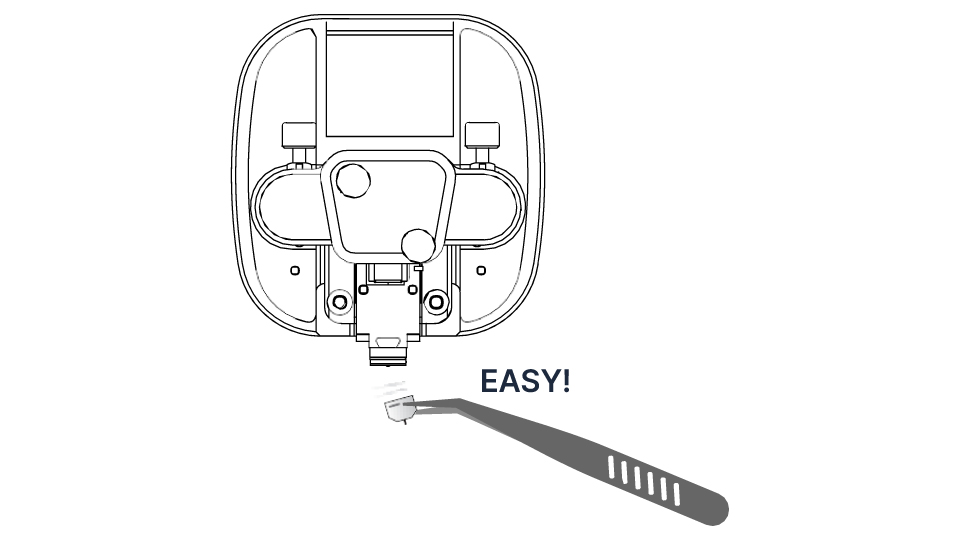
Pre-Mounted Probe
AFM probe exchange can be challenging, even for experienced users, often resulting in cantilever breakage. Park AFM addresses this by using pre-aligned probe chip carriers with kinematic mounting points, ensuring reliable and consistent tip positioning.
The NX head Z scanner features three precision balls for kinematic mounting, complemented by magnets at the base to ensure a secure, reliable, and repeatable mounting position.
Improved Z Scan Straightness
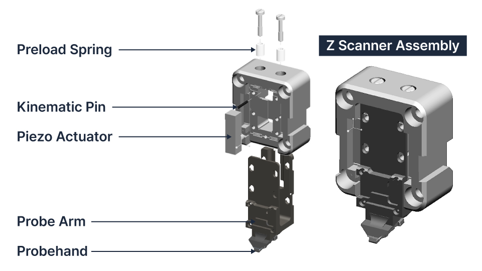
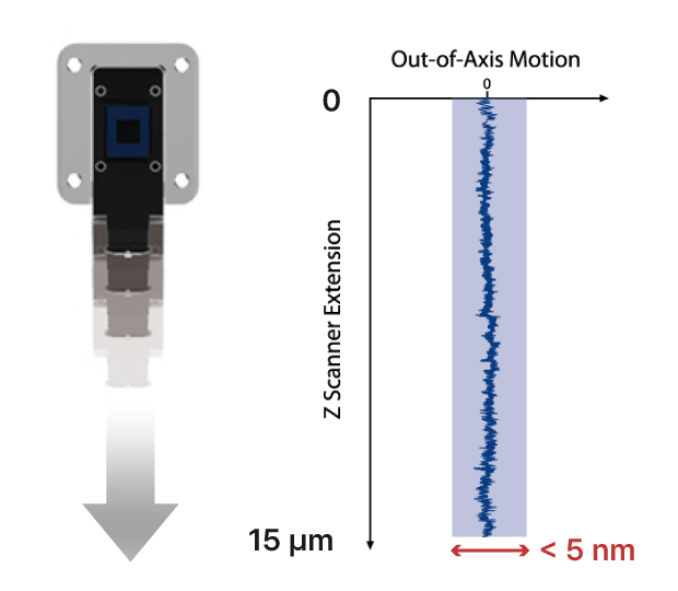
Park NX series Z scanner maintains straightness within 0.1% across the usable range, with out-of-axis motion under 5 nm even at a full 15 µm extension.
Its compact assembly, combining a preload spring, kinematic pin, and piezo actuator, minimizes drift and ensures accurate vertical motion for reliable, distortion-free nanoscale measurements.
Simple Expansion Slot for Modes and Options
Simply plug an option module into the expansion slot to enable advanced AFM modes. Park NX series AFM features a modular design, ensuring compatibility with options across its product line.
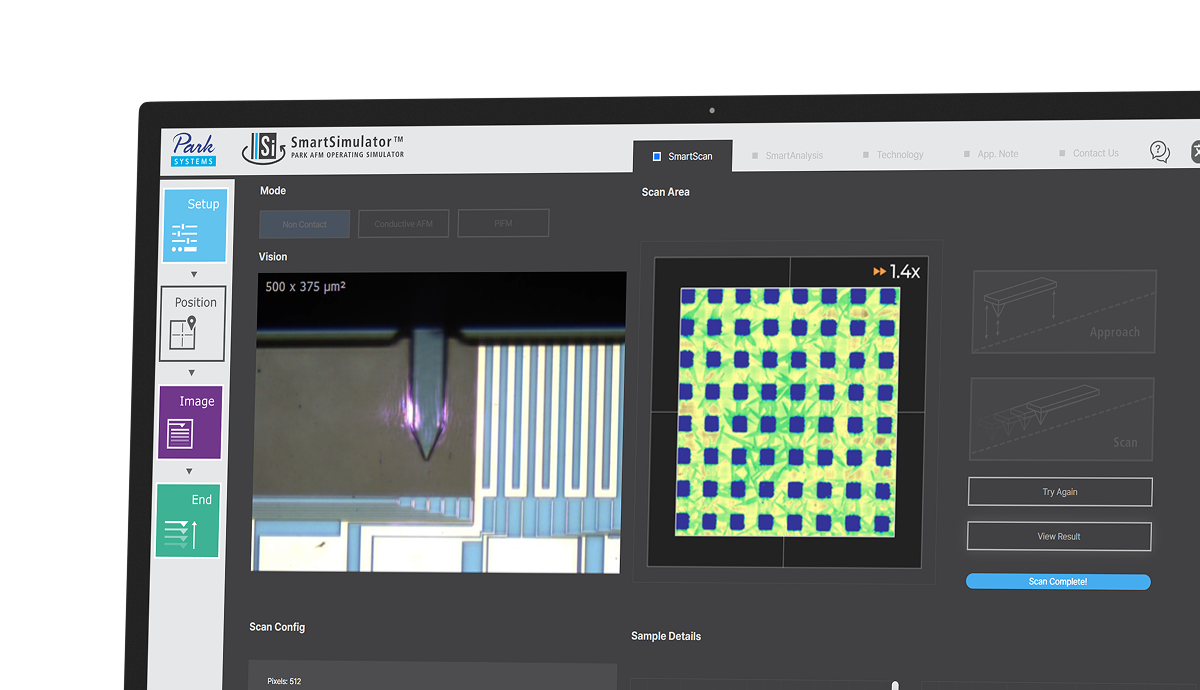
On-Axis Optical Microscope
The high-power on-axis optical microscope provides a clear view of the sample surface. A software-controlled LED light source illuminates the sample surface for better observation.
Park AFM Technology
Orthogonal Scan System
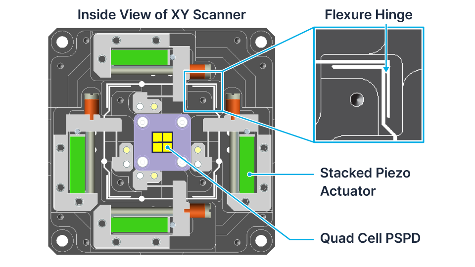
Conventional AFMs with tube scanners suffer from out-of-plane motion and axes crosstalk, resulting in image distortion, especially over large scan areas. NX10, like all Park AFMs, employs an advanced orthogonal scan system featuring a flexure-guided architecture: a 2D flexure scanner moves the sample in the XY plane, while a separate 1D flexure scanner independently controls the probe’s Z-axis motion. This separated scanner system ensures highly orthogonal, linear scans with minimal out-of-plane motion and fast dynamic performance.
The XY scanner is designed to achieve flat, purely horizontal motion without vertical interference by using stacked piezo actuators and flexure hinge structures. A position sensor is located at the center of the scanner to provide direct feedback for servo control, minimizing positioning errors across the scan area. This design ensures consistent accuracy and stability, even when scanning large samples.
Park AFM Technology
True Non-Contact™ Mode
NX10 features True Non-contact™ mode, a proprietary technology exclusively offered by Park Systems. True Non-contact mode obtains topography by detecting the attractive van der Waals force between the AFM tip and the sample surface.