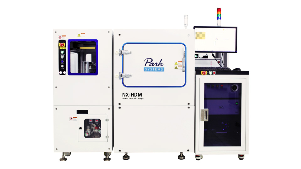
Park NX-HDM is a leading-edge atomic force microscope (AFM) purpose-built for semiconductor R&D, FA, and QA laboratories, supporting wafers up to 150 mm. Leveraging Park Systems’ proven AFM technology, it delivers advanced measurement capabilities for semiconductor process development, failure analysis, and quality control, with full SEMI standards compliance and complete automation.
Widely adopted by major semiconductor manufacturers worldwide, its proven track record stands as a testament to the system’s reliability and effectiveness in semiconductor metrology
Key Features
Automated Operation
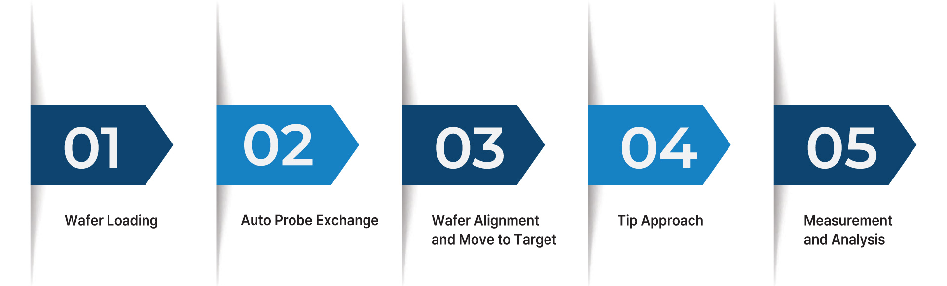
The NX-HDM enables fully automated operation from wafer handling to measurement and analysis. It automatically receives a recipe from a host, performs end-to-end automation by selecting the appropriate tip, scanning multiple target areas, analyzing the data, and generating reports.
Automated Wafer Handling Capability
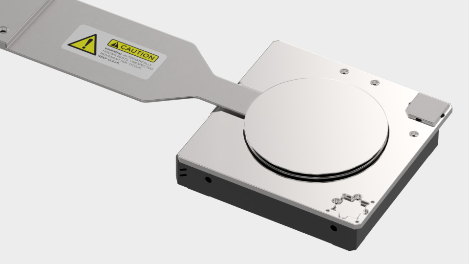
Wafer transfer is performed automatically by an equipment front end module (EFEM) equipped with a single loadport. It uses robotic mechanisms, sensors, and algorithms to ensure precise alignment and safe, reliable handling of wafers of various sizes and materials.
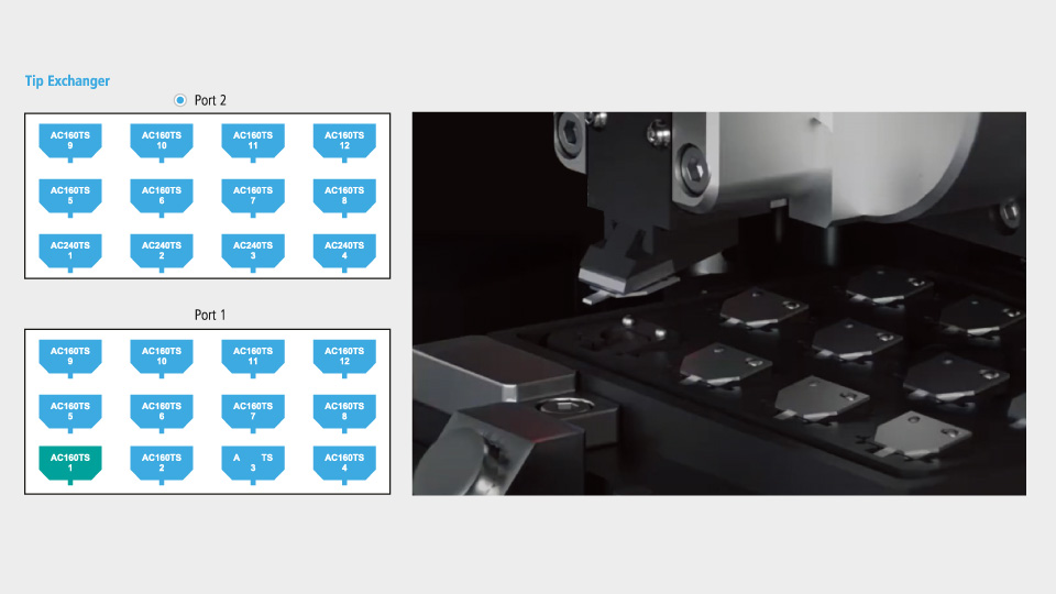
Automatic Probe Exchange
The automatic tip exchanger seamlessly replaces the probe when a threshold is exceeded. It can store up to 24 pre-mounted probes (12 probes per cassette).
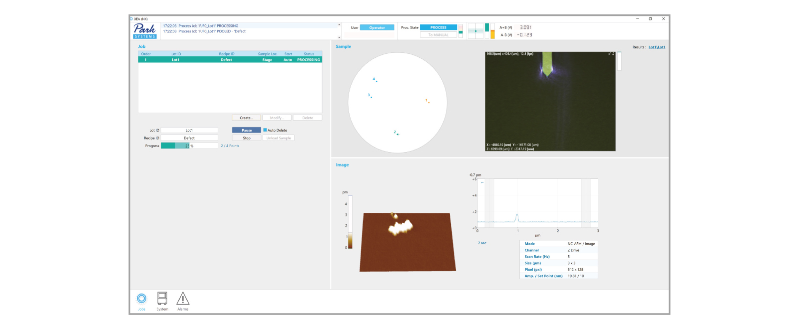
Automatic Measurement Control for Accurate Scans with Minimal Effort
Park NX-HDM is equipped with automated software that makes operation nearly effortless. Simply select the desired measurement program to get precise multi-site analysis with optimized settings for cantilever tuning, scan rate, gain, and setpoint parameters. Park’s user-friendly software interface gives you the flexibility to create customized operation routines, allowing you to access the full power of the NX-HDM and get the measurements you need. Creating a new routine is straightforward — it takes about 10 minutes from scratch, or less than 5 minutes to modify an existing one.
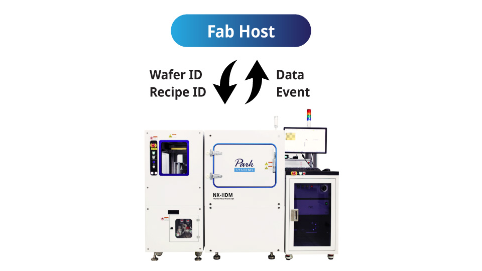
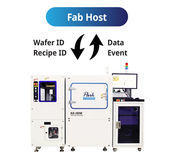
Fab Host Communication via SECS/GEM Protocol
The system enables Fab host communication via the SECS/GEM protocol, ensuring full compliance with SEMI standards, including E30, E40, E87, E90, E94, and E84 PI/O for AMHS integration. (Available when EFEM option is installed)
Park AFM Technology
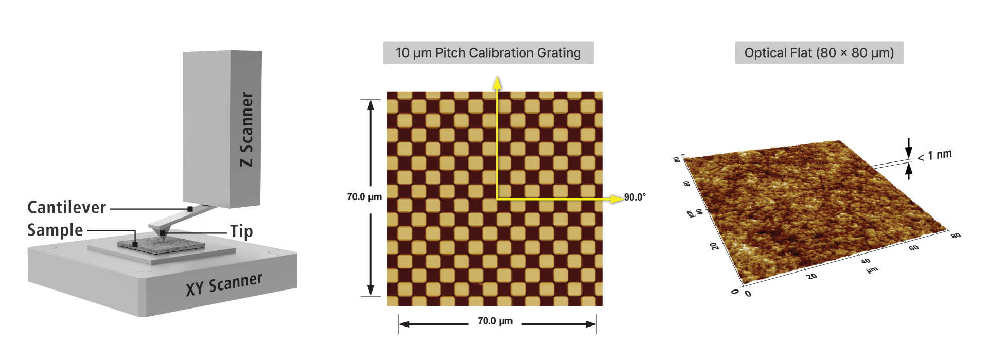
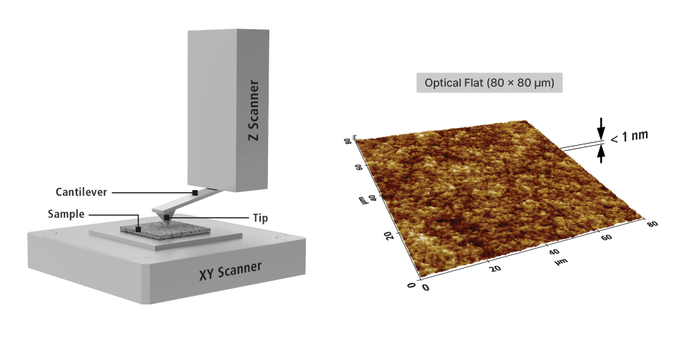
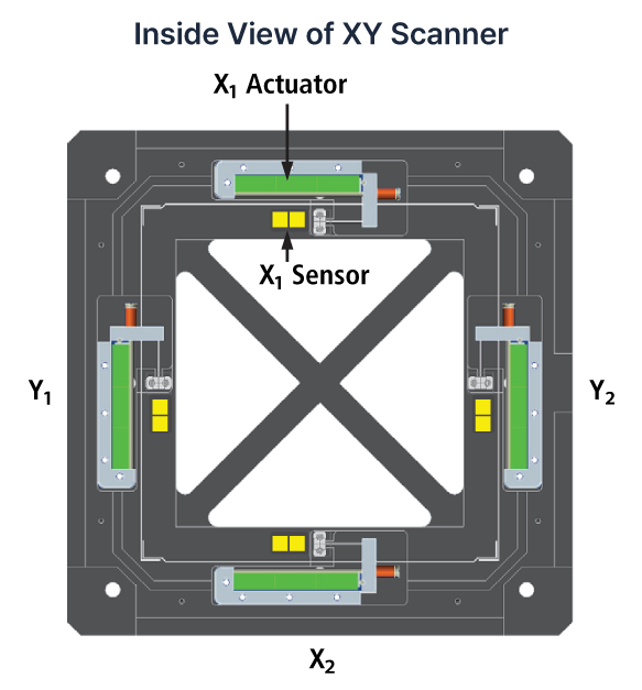
Orthogonal Scan System
The separated flexure-guided 2D XY scanner and 1D Z scanner system minimizes out-of-plane motion by eliminating crosstalk between horizontal and vertical motion. The independent Z scanner enables precise, linear, and fast dynamic performance.
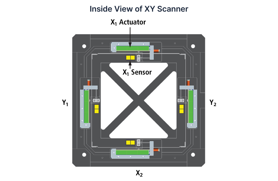
The XY scanner features a dual-servo architecture with two pairs of actuators and position sensors mounted on opposite sides of each axis, providing
precise orthogonality and accurate positioning across the entire scan area.
Park AFM Technology
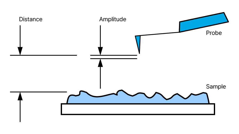
True Non-Contact™ Mode
True Non-contact™ mode, a proprietary technology offered by Park Systems, obtains topography by detecting the attractive van der Waals force between the tip and sample surface. The key advantage of True Non-contact mode is the prevention of tip wear and sample damage, ensuring consistent results with superior data reliability. This also reduces the total cost of ownership by extending tip life.
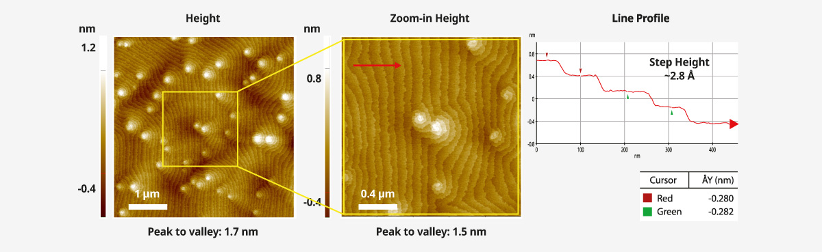
Sub-Nanometer Step Height Measurement of GaN Epi Film on Si Substrates
GaN epitaxial films grown on Si substrates are used in LED and power electronic devices. Non-contact mode provides height images that reveal step-terrace surface topography on the GaN film, and line profiles show sub-nanometer step heights between terraces.
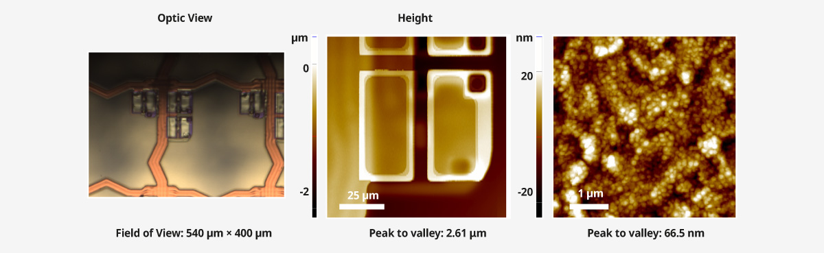
Nanoscale Roughness Measurement for Micro-LED
Micro LED is a self-emissive display device used for high-brightness, high-resolution applications such as AR/VR and next-generation mobile displays. Non-contact mode provides height and zoom-in images that resolve nanoscale roughness (~66 nm peak-to-valley) and surface morphology of each cell, supporting detailed inspection during device development.
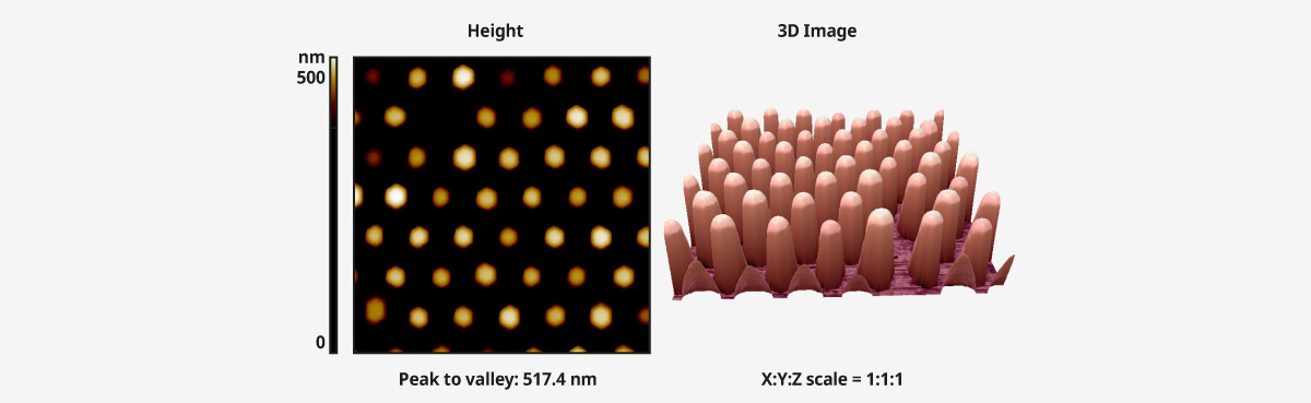
3D Image of Gallium Nitride (GaN) LED Wire Arrays
GaN nanowire LED structures consist of vertically oriented GaN nanowire arrays, which are commonly studied as model structures in nanoscale optoelectronic devices to examine their geometric and structural characteristics. Height and 3D images acquired in Non-contact mode show the array geometry, providing information on the spatial arrangement and height variations of the nanowires across the scanned area.