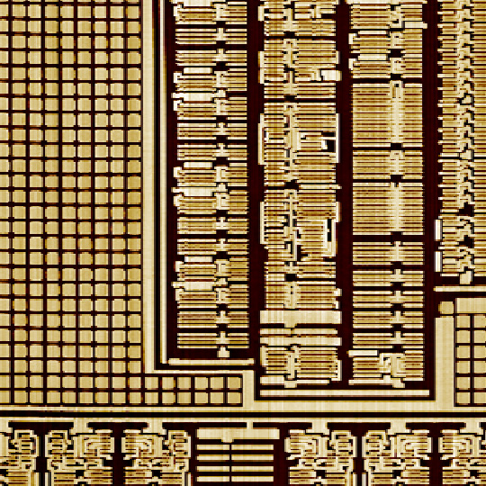
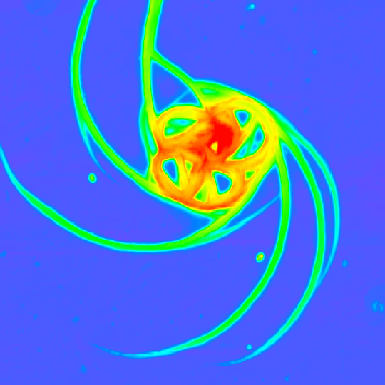
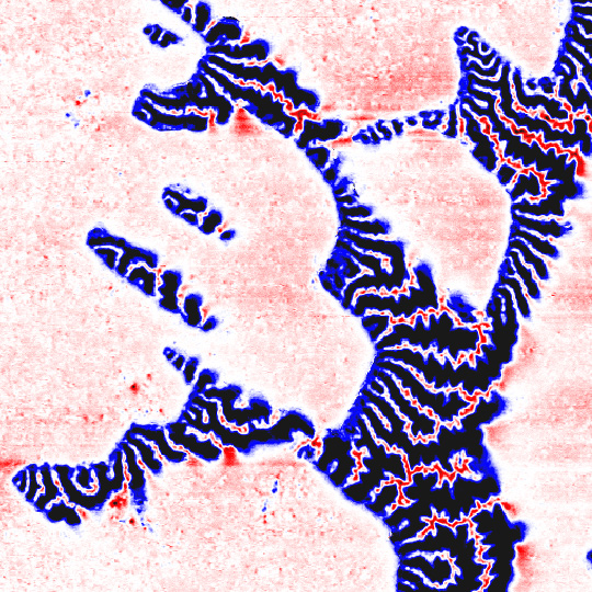
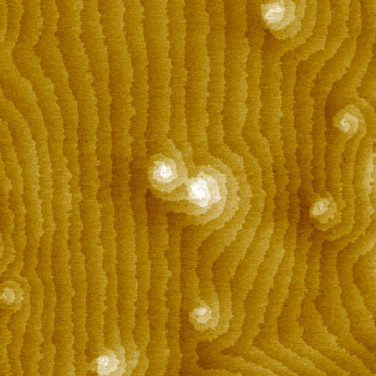
| Contact Us   Global
×

Error

An error has occurred.
Report image

If you found this image unacceptable, please let us know. We will review your report and take action if we determine this image is really unacceptable.

Please enter your name
Please enter your comment

Trench Etch Profile on Si Wafer

Trench Etch Profile on Si Wafer

Top dielectric trench etch profile on Si wafer having tapered slope at the trench sidewall.

Scanning Conditions

- System: NX20
- Scan Mode: Non-contact
- Cantilever: AC160TS (k=26N/m, f=300kHz)
- Scan Size: 3μm×3μm
- Scan Rate: 0.21Hz
- Pixel: 1024 × 256