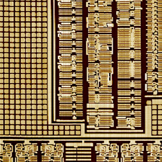
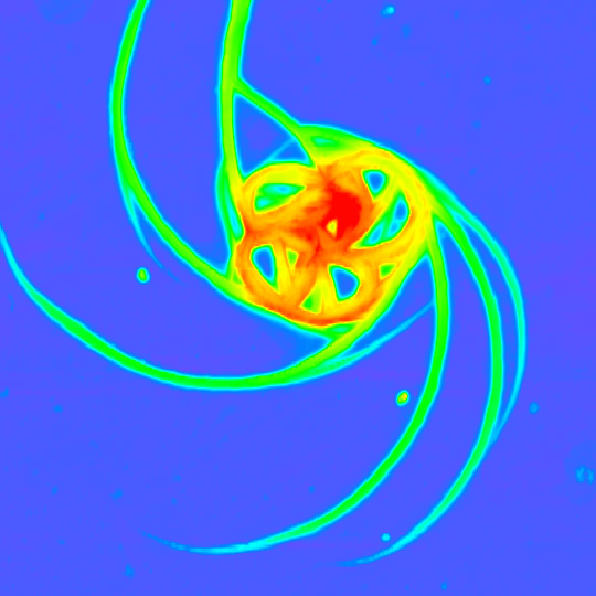
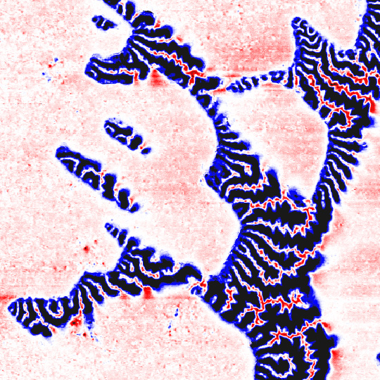
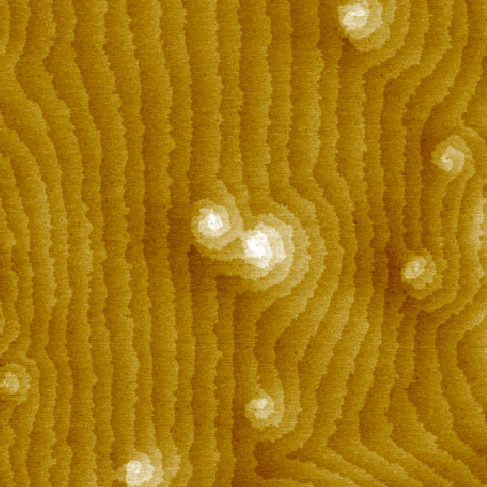
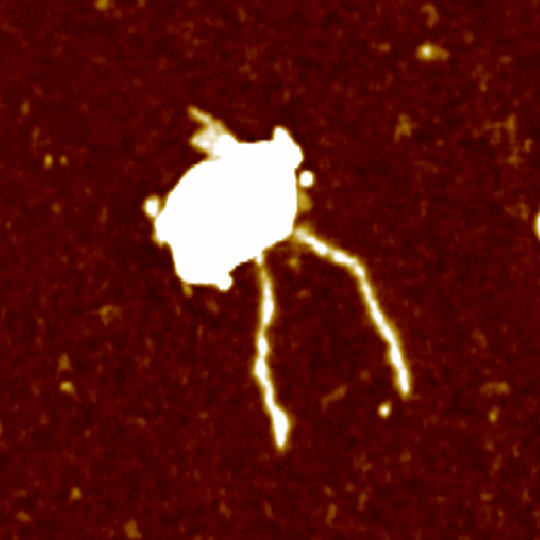
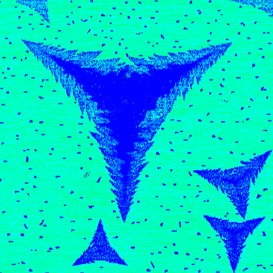
-
solar_cell AdhesionForce Platinum Piezo Copper polyvinyl acetate SrO LiquidCrystal Hafnium_dioxide lithography Fendb dielectric_trench Treatment AtomicLayer ThermalConductivity LifeScience PolymerPatterns Gallium #EC Trench phase_change temp_control ConductiveAFM DIWafer Regensburg cannabis ScanningIon-ConductanceMicroscopy FM-KPFM NanoLithography PolyvinylAcetate ScanningTunnelingMicroscopy F14H20 molecular_self_assembly Magnets SPMLabs
Report image
If you found this image unacceptable, please let us know. We will review your report and take action if we determine this image is really unacceptable.
MoS2 Layers on SiO2
Scanning Conditions
- System: NX10
- Scan Mode: Non-contact
- Cantilever: AC160TS (k=26N/m, f=300kHz)
- Scan Size: 5μm×5μm
- Scan Rate: 1Hz
- Pixel Size: 256 × 256
- Scan Mode: Non-contact
- Cantilever: AC160TS (k=26N/m, f=300kHz)
- Scan Size: 5μm×5μm
- Scan Rate: 1Hz
- Pixel Size: 256 × 256