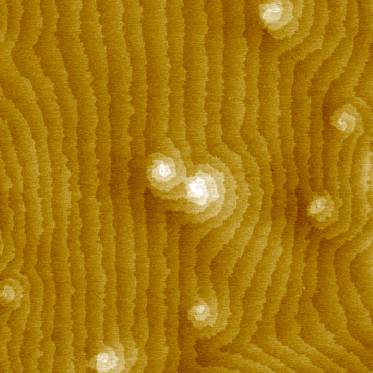
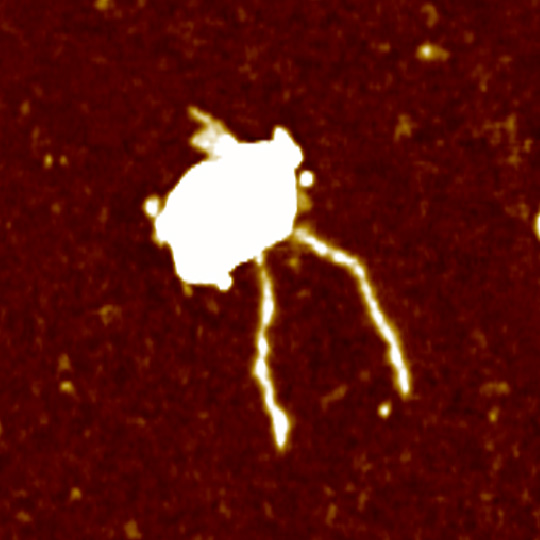
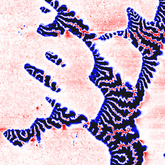
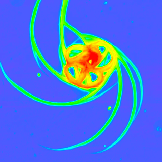
Your current characterization methods may show you what your sample looks like—but what about the nanoscale details you may be missing?
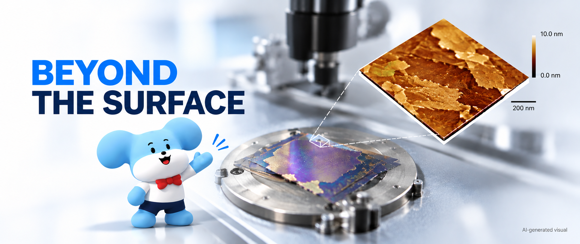
When surface morphology, roughness, topography, or local material properties matter, AFM can add another dimension to your analysis.
Different characterization techniques reveal different aspects of your samples. AFM complements these methods by providing nanoscale surface details and quantitative measurements that add new insights to your research.
Optical Microscopy
What You Already See
Large-area views of samples, including overall morphology, visible features, and regions of interest.
What AFM Can Add
Nanoscale surface details, quantitative height measurements, and localized surface-property characterization.
Scanning Electron Microscopy (SEM)
What You Already See
High-resolution images of surface morphology, including particles, grains, and fine structural features.
What AFM Can Add
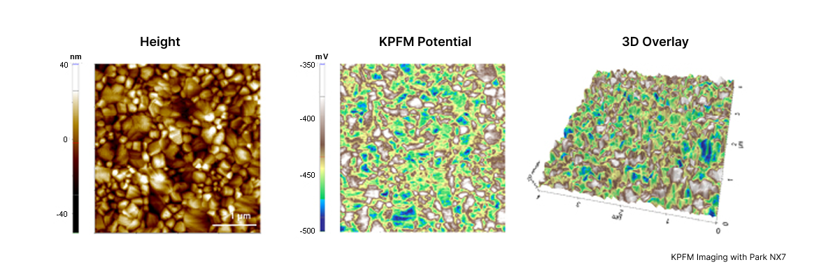
Quantitative 3D topography, localized mechanical and electrical properties, and nanoscale roughness.
Profilometry
What You Already See
Surface profiles, step heights, waviness, and roughness measurements across relatively large areas.
What AFM Can Add
High-resolution 3D surface topography, localized nanoscale roughness, and detailed surface-feature analysis.
How Does AFM Work?
AFM uses a sharp probe to scan across a sample surface and detect interactions between the probe and the sample. These measurements are transformed into a high-resolution, three-dimensional map of the surface.
Scan the Surface: A sharp probe scans across the sample surface to collect data.
Measure Surface Properties: Probe–sample interactions are used to measure surface height and other material properties.
Build a 3D Surface Map: The collected measurements are used to create a detailed 3D map of the surface.
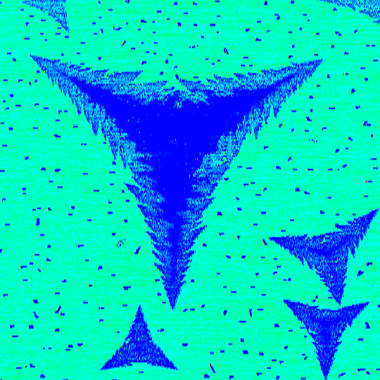
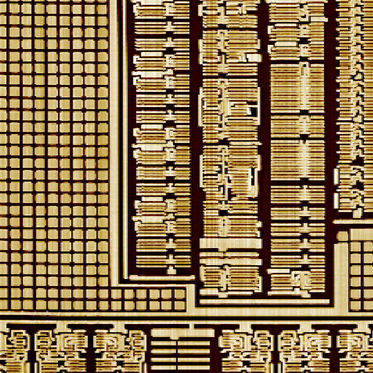
Across semiconductors, advanced materials, and biological samples, AFM can add a new dimension to your existing characterization workflow—revealing nanoscale morphology, topography, and local properties that conventional techniques may not fully capture.
Ready to Explore the Nanoscale? Start with Park NX7.
Park NX7 brings high-resolution AFM imaging into a compact, user-friendly tabletop system, making nanoscale surface characterization more accessible across diverse applications.
High-resolution imaging with fast Z-servo performance
True Non-contact™ technology for tip and sample protection
Inspire the next generation of researchers with hands-on AFM experience. Park Systems is working to make hands-on AFM learning more accessible with NX7.
Contact us to explore options for your institution.