

Jinpeng Xu, a Research Assistant at the Institute of Physics, Henan Academy of Sciences, has recently made a key breakthrough in polarity control of transition metal dichalcogenides (TMDs), addressing the long-standing challenge of achieving stable p-type behavior in these materials.
His work, entitled “Polarity-Modulated p-Type WS₂ Nanotube Thickets for High-Performance Photodetection,” was published in Advanced Functional Materials (DOI: https://doi.org/10.1002/adfm.75293). Xu and his colleagues report a morphology-driven strategy for polarity modulation through the synthesis of WS₂ nanotube thickets (NTTs) on SiO₂/Si substrates using a simple, cost-effective Au nanoparticle-catalyzed chemical vapor deposition process. This previously unreported interlaced nanotube architecture enables scalable growth while intrinsically driving WS₂ into a robust p-type state, overcoming its native n-type nature without any external doping or surface treatment.
Based on this material, field-effect transistors display a hole mobility of 0.26 cm² V⁻¹ s⁻¹ and excellent photodetection at 650 nm over a wide temperature range of 10–300 K under high vacuum (5 × 10⁻⁵ mbar). The device achieves a responsivity of 2.7 × 10⁴ A W⁻¹, an external quantum efficiency of 6.3 × 10⁶%, and a detectivity of 1.6 × 10¹³ Jones, with rise and fall times of 13 ms and 22 ms, respectively. Demonstrations in imaging, optical communication, and digit recognition confirm the versatility of this platform.
This breakthrough opens a new avenue for TMD optoelectronics, innovatively proposing that nanotube morphology itself can serve as a built-in polarity-control knob, rather than relying on external doping or post-treatment. This concept is expected to be extendable to other TMD materials and nanostructure systems, laying an important foundation for morphology-driven polarity engineering in two-dimensional optoelectronic devices.
1. Please summarize the research you do and explain why it is significant?
Two-dimensional (2D) material photodetectors show great promise for optical communications, intelligent imaging, and information processing. However, their intrinsic n-type characteristics severely restrict the development of high-performance p-type devices. To address this challenge, we synthesized a novel WS2 nanotube thickets (NTTs) structure on SiO2/Si substrates via Au-nanoparticle-catalyzed chemical vapor deposition. Composed of densely intertwined multi-walled nanotubes, the NTTs form a 3D network with built-in strain fields, abundant interface states, and strong inter-tube coupling. This unique “nanotube thicket” morphology reshapes not only the geometric structure but also the electronic structure at the microscopic level, spontaneously converting WS2 from intrinsic n-type to stable p-type conduction without any external doping or surface treatment.
Combined with temperature-dependent electrical measurements and first-principles calculations, this study reveals that curvature-induced strain, inter-tube coupling, and interface states in NTTs act synergistically to rearrange the band structure and shift the Fermi level toward the valence band, thereby stabilizing p-type transport. Phototransistors based on WS2 NTTs exhibit a responsivity of 2.7×10⁴ A W⁻¹, a specific detectivity of 1.6×10¹³ Jones, and an external quantum efficiency of 6.3×10⁶ % under 650 nm laser illumination. Furthermore, the devices operate stably over a wide temperature range of 10–300 K and have been successfully validated in imaging and optical communication applications, demonstrating excellent application potential. This work provides a universal and scalable strategy for controllable polarity modulation in 2D semiconductors and is expected to advance the practical application of 2D materials in next-generation optoelectronic devices.
2. How might your research be used?
Our research provides a new strategy for next-generation high-performance p-type transition metal dichalcogenides (TMDs) optoelectronic devices, mainly in three aspects:
First, semiconductor polarity modulation: The proposed morphology-induced strain approach stably converts intrinsic n-type WS2 to p-type conduction without external doping or surface treatment, offering a scalable physical mechanism and fabrication solution to the critical bottleneck of realizing stable p-type transport in TMDs.
Second, 2D material complementary electronics: Field-effect transistors based on intrinsic p-type WS2 NTTs show reliable hole-transport characteristics and can be integrated with conventional n-type TMD devices, supplying key material support for low-dimensional CMOS circuits, p–n heterojunctions, and complementary optoelectronic integrated systems.
Third, broadband, wide-temperature photodetection: The fabricated photodetectors respond from the ultraviolet–visible to near-infrared regions and operate stably from 10 to 300 K. With high responsivity, high detectivity, and low dark current, they are suitable for weak-light detection, low-temperature sensing, visible light communication, and high-resolution imaging.
3. Why is the Park AFM important for your research?
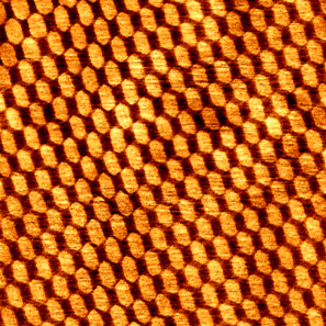
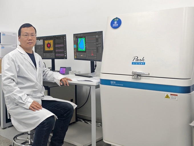
Park AFM is indispensable and irreplaceable for this research, serving as the core characterization tool for revealing the intrinsic relationship among the morphology, electronic structure, and transport polarity of WS2 nanotube thickets. On the one hand, its high-precision topography imaging and thickness measurement accurately capture the surface morphology, uniform distribution, and thickness of the NTTs, directly providing critical structural evidence for the core scientific mechanism of “curvature-induced strain–polarity modulation”. On the other hand, its KPFM function for surface potential and work function measurement precisely determines the work function and interfacial potential distribution, offering decisive electronic evidence for clarifying p-type transport, band alignment, and metal–semiconductor contact characteristics.
In addition, the high sensitivity and multi-mode integration of Park AFM allow topographic and electronic characterization on a single platform, avoiding errors caused by switching between multiple instruments and greatly improving experimental efficiency and data reliability. In summary, Park AFM fully supports the entire chain of analysis from microstructure to electronic properties, making it an essential instrument for verifying the core scientific findings and completing the mechanistic interpretation of this study.
4. What features of Park AFM are the most beneficial and why?
The high-spatial-resolution imaging and surface potential measurement of Park AFM are essential characterization tools in this study. Its precise imaging accurately characterizes the morphology, thickness, and microstructure of the materials, providing structural evidence for curvature-induced strain and polarity modulation. The KPFM mode measures the surface potential and work function of the material, offering key electronic evidence for p-type transport behavior and band alignment.
%20Webinar.png)