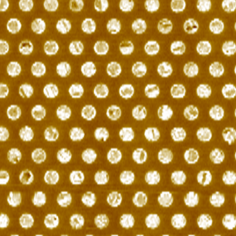
Speaker : Phil Kaszuba Affiliation : Senior Member of Technical Staff and Lead Engineer, SPM Laboratory, Global Foundries, ASM Fellow Region : LatAm Year : 2021 Language : English Explore the applications of Scanning Probe Microscopy (SPM) in semiconductor analysis. From topographic assessment of silicon structures to detecting defects and stress lines at the nanoscale, delve into examples showcasing how SPM techniques such as Atomic Force Microscopy (AFM), Scanning Kelvin Probe Microscopy (SKPM), and Scanning Capacitance Microscopy (SCM) contribute to advanced semiconductor analysis, offering insights from early development to failure analysis and addressing challenges in state-of-the-art technologies.