Abstract
Torsional Force Microscopy (TFM) is an advanced AFM technique specifically designed for detecting dynamic frictional forces at the nanoscale. It is highly effective for revealing both moiré superlattices and atomic lattices in van der Waals (vdW) heterostructures.
These include bilayer graphene and graphene/hexagonal boron nitride (hBN) systems, where subtle variations in twist angle can significantly alter electronic properties. TFM does not require electrical contact between the probe and the sample, making it suitable for characterizing insulating or floating structures. It offers researchers a powerful, non-invasive method to examine 2D materials on polymer substrates, even during intermediate fabrication stages, under ambient conditions. This application note introduces the principles of TFM and demonstrates its capability using the Park FX40 AFM system.
Introduction
Torsional Force Microscopy (TFM) is a specialized mode of atomic force microscopy (AFM) that enables sensitive detection of dynamic lateral forces at the nanoscale. This technique is particularly effective for visualizing moiré superlattices and atomic lattices within van der Waals (vdW) heterostructures, such as bilayer graphene and graphene/hexagonal boron nitride (hBN) stacks. In these systems, even slight changes in the interlayer twist angle can lead to dramatic modifications in their electronic behavior1,2.
Unlike many conventional AFM-based techniques, TFM does not require an electrical connection to the sample or the probe, making it ideal for examining electrically insulating or floating structures. Its ability to operate in ambient conditions and to resolve both surface and shallow subsurface structural features allows researchers to investigate two-dimensional (2D) materials supported on soft polymer substrates, including those in intermediate stages of fabrication.
Moiré superlattices result from the stacking of two layers of graphene or other 2D materials at a small twist angle. While these structures have been widely explored due to their unique physical properties, direct imaging methods under ambient conditions — specifically in air and at room temperature — remain limited3. Even slight variations in twist angle, on the order of hundredths of a degree, can drastically alter the electronic characteristics of these systems2. Although various imaging approaches have been developed, most require complex instrumentation, extensive post-synthesis processing, or both. In practice, moiré superlattices
often suffer from inconsistent twist angles and poor spatial uniformity, posing significant challenges for reproducible fabrication and characterization4. To support the optimization of heterostructure assembly, there is a strong demand for an imaging technique that is fast, accessible, and reliable. Such a method should function in ambient environments, without the need for electrical connections or surface modification, and be compatible with partially assembled van der Waals stacks on polymer substrates commonly used in stacking processes. This work presents the need for such a rapid and practical feedback solution and introduces
TFM as a method that addresses these critical requirements.
Park Systems has recently implemented TFM to provide researchers with access to this advanced technique. In this application note, we present representative TFM data acquired from 2D material samples using the next-generation research automated AFM, Park FX40, along with details on the system’s hardware configuration optimized for TFM measurements.
Various SPM applications for imaging moiré superlattices
Several scanning probe microscopy techniques have been explored to visualize moiré patterns and atomic lattices in 2D materials.
Conductive AFM (C-AFM) allows atomic resolution imaging but requires conductive samples and substrates5. Amplitude-modulation AFM (AM-AFM), including tapping mode, can face challenges in clearly resolving fine moiré contrasts, unlike contact mode, which typically provides better contrast6. Scanning microwave impedance microscopy (sMIM) offers non-contact measurements but lacks atomic resolution7. Among these, Lateral Force Microscopy (LFM) and Friction Force Microscopy (FFM) have been effective for visualizing both moiré and atomic-scale structures in materials such as hBN and graphite8,9. However, their ability to detect subsurface structures remains unproven. TFM addresses this gap by utilizing torsional resonance modes, enabling high-sensitivity mapping of frictional contrast and thus offering clearer visualization of moiré structures across varying depths.
To replicate high-resolution maps comparable to those previously achieved by various techniques, torsional resonances sensitive to dynamic friction at the AFM tip-sample interface were employed. This proved highly effective for clearly resolving moiré contrast or even atomic lattices.
Fundamentals of TFM
TFM operation involves two simultaneous control schemes. First, closed-loop feedback tracks the sample topography, maintaining a constant normal loading force. Concurrently, an open-loop excitation at the cantilever’s torsional resonance is applied to detect variations in lateral friction. This dual-mode configuration ensures high frictional contrast by combining sensitive torsional excitation with stable tip-sample contact control. To induce pure torsional motion without introducing vertical or flexural artifacts, a pair of bimorph actuators is driven exactly 180° out of phase. This symmetric configuration ensures that vertical displacements
are canceled out while generating a clean rotational torque at the cantilever base, thereby selectively exciting the torsional eigenmode with high efficiency. A single bimorph or asymmetrical drive would also excite non-torsional modes and reduce signal clarity due to mechanical cross-talk and mode mixing. The lateral deflection resulting from this controlled torsional excitation is then monitored to map nanoscale frictional variations. These signals, when analyzed across torsional resonances, provide high-resolution information about surface and subsurface structures without the need for electrical biasing.
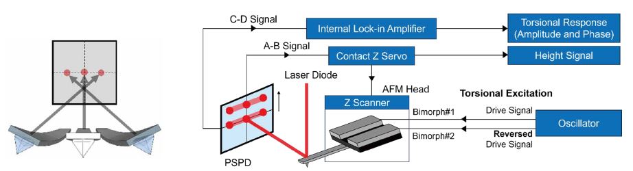
Figure 1. Simplified schematic overview of TFM operation. A closed-loop feedback maintains topography tracking, while torsional resonance is excited through paired out-of-phase piezo drives. Lateral deflection signals reveal frictional contrast across the scanned surface.
TFM builds upon a two-mode control scheme that combines vertical feedback and lateral torsional excitation to detect nanoscale frictional variations with high spatial resolution. As illustrated in Figure 1, the system simultaneously maintains topographic tracking through closed-loop control while driving the cantilever's torsional resonance via open-loop excitation. To ensure stable imaging conditions throughout the scan, the vertical Z-feedback maintains a constant normal force by adapting to the surface contours of the sample, following the principle used in conventional contact-mode AFM.
Torsional excitation is achieved by applying 180° out-of-phase signals to a pair of piezo actuators integrated into the cantilever holder, generating a rotational drive around the cantilever’s long axis. The lateral deflection is detected by the photodetector’s side quadrant channel (the PSPD), and its amplitude near the torsional resonance frequency indicates local variations in friction.
By scanning across the surface while maintaining this torsional excitation, TFM effectively maps nanoscale variations in friction linked to structural features such as moiré patterns or atomic lattices. Since the technique does not rely on electrical biasing or contact-based charge transfer, it avoids issues like electrostatic interference or sample charging. This makes TFM particularly well-suited for characterizing electrically insulating or floating samples, as well as fragile 2D materials or partially fabricated heterostructures.
By combining vertical force stability with lateral resonance sensitivity, TFM provides a powerful and non-invasive method for revealing fine mechanical contrasts in complex nanoscale systems, supporting advanced surface and interface characterization.
High-resolution TFM Imaging of Moiré Patterns and Atomic Lattices
To demonstrate the capabilities of TFM, high-resolution imaging was performed under ambient conditions on a variety of van der Waals (vdW) heterostructures, including a cleaved (001) surface of muscovite mica, single-layer graphene on hexagonal boron nitride (Gr/hBN) and twisted bilayer graphene (tBG). The results demonstrate TFM’s ability to resolve both moiré patterns and atomic lattices with high spatial precision across multiple scales.
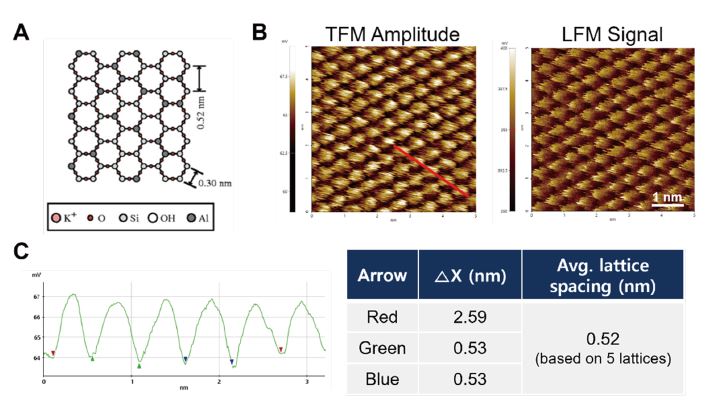
Figure 2. High-resolution images of mica surface measured by LFM and TFM. (A) The crystal structure schematic of a cleaved mica surface with its lattice spacing distance. (B) Comparative images of mica surface (101) acquired with TFM and LFM modes. (C) Line profile of TFM image. The corresponding LFM and TFM measurement conditions were as follows: cantilever PPP-FMR, 512 × 512 pixel, scan rate of 8 Hz, and scan size 5 × 5 nm².
TFM was also applied to a cleaved (001) mica surface to examine atomic lattice-level contrast. As shown in Figure 2, TFM clearly resolved periodic atomic-scale features, whereas LFM measurements at the same location resulted in noisy images with less distinctive structure and frequent spike-like artifacts at specific direction. The superior sensitivity of TFM to lateral friction enabled clean visualization of atomic lattice contrast even at the small scan size of 5 × 5 nm². Further, the TFM data proved its measurement accuracy by matching its atomic lattice periodicity, which is very closely matched with reported value10, 0.52 nm.
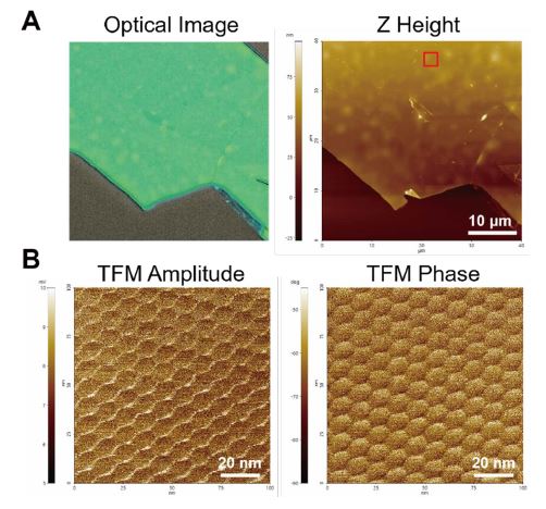
Figure 3. (A) Optical and large-area topography image of single graphene layer on hBN. (B) High-resolution TFM image acquired from the zoomed-in region marked by the red square in (A). The corresponding TFM measurement conditions were as
follows: cantilever AD-2.8-AS, 512 × 512 pixel, scan rate of 3 Hz, and scan size at 100 × 100 nm².
Figure 3 shows the TFM results obtained on a single graphene layer on hBN (Gr/hBN). The optical image and wide-area topography (40 × 40 μm²) confirm the multilayered structure. In the high-resolution small scans (100 × 100 nm²), TFM clearly resolved moiré contrast linked to the twist angle.
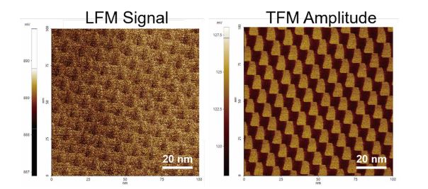
Figure 4. TFM and LFM images of twisted bilayers of graphene. TFM reveals clear moiré lattice periodicity, while LFM exhibits poor resolution and high background noise. The corresponding LFM and TFM measurement conditions were as follows: cantilever Scout 70, 512 × 512 pixel, scan rate of 4 Hz, and scan size at 100 × 100 nm².
TFM was also applied to a twisted bilayer graphene sample to visualize the resulting moiré patterns. As shown in Figure 4, TFM clearly resolved the periodic features, whereas LFM measurements at the same location produced noisy images with poorly defined structures. The superior lateral friction sensitivity of TFM enabled clean and distinct visualization of the moiré pattern contrast.
Conclusion
Torsional Force Microscopy (TFM), as implemented on the Park AFM systems, provides a powerful and reliable method for high-resolution imaging of moiré superlattices and atomic lattices in 2D materials under ambient conditions. By detecting lateral frictional variations without the need for electrical contacts or sample conductivity, TFM enables direct and very minimally invasive visualization
of both surface and shallow subsurface structural features. This capability is particularly valuable for characterizing twisted heterostructures, where subtle differences in twist angle and interlayer coupling critically influence material properties. The high spatial sensitivity, ambient operability, and compatibility with soft or insulating substrates make TFM a practical and versatile tool for both research and process monitoring.
As interest in 2D quantum and electronic materials continues to grow, TFM is expected to serve as a valuable technique for providing structural insight and supporting the development of next-generation devices.
Application
Related Products
Related Contents
Solving Thin-Film Uniformity Challenges on Curved Surfaces with Imaging Spectroscopic Ellipsometry
Spectroscopic Imaging Ellipsometry at Cryogenic Temperatures Applied to Atomically Thin Crystals