- Journal: Nano Letters
- Published Year: 2024
- Authors: Ian Sequeira, Andrew Z. Barabas, Aaron H Barajas-Aguilar, Michaela G Bacani, Naoto Nakatsuji, Mikito Koshino, Takashi Taniguichi, Kenji Watanabe, and Javier D. Sanchez-Yamagishi
- Application: graphene, 2D materials nanomanipulation, van der Waals materials, electronic devices
Summary
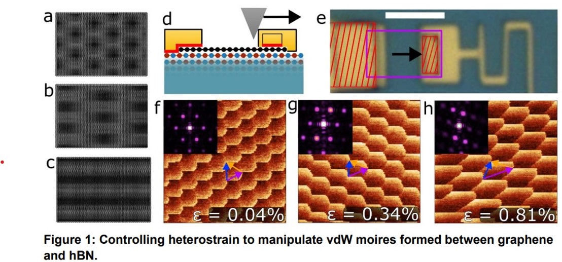
In this paper, researchers demonstrate a method to controllably introduce in-situ large heterostrain in graphene-hexagonal boron nitride (g-hBN) devices and study its effects on moire structure and transport properties. Devices were fabricated in such a way as to have a sliding electrode attached to the top graphene layer that could be moved with an AFM probe. While performing simultaneous electrical measurements, they apply large strain directly to a monolayer of graphene (>1%) without straining the substrate (hexagonal boron nitride). To image the effects of heterostrain on the g-hBN moire, they perform conductive AFM (C-AFM) on the Park NX10 AFM.
This innovative approach opens the doors for nanomanipulation of other heterostructures to precisely tune their electrical properties and expand the possibilities for these devices to be used in commercial applications.