


Logic Wafer


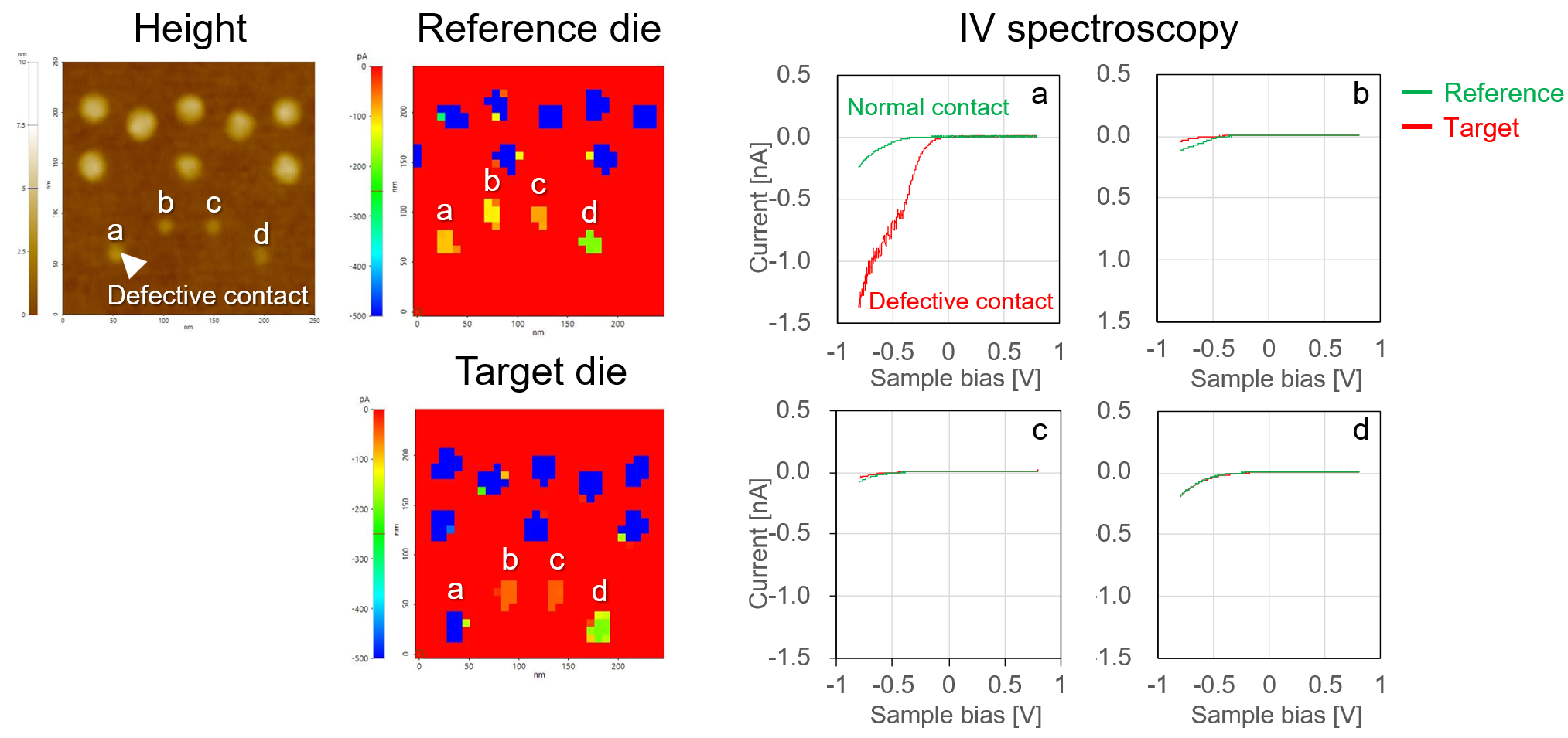
Two dies on a logic wafer are analyzed to evaluate electrical behavior at individual contacts.
Conductive AFM IV mapping identifies defective contacts by comparing local electrical behavior at each die and contact site, enabling rapid defect screening and wafer-level process monitoring.
Scan Conditions
- System: NX-eView
- Scan Mode: IV Mapping
- Scan Size: 250 nm×250 nm
- Scan Rate: 0.8 Hz
- Pixels: 256×64
- Cantilever: AD-40-SS
(k=40 N/m, f=180 kHz)
- Sample Bias: -0.8 V – +0.8 V
Application
×