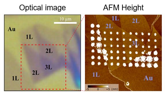
MoSe₂ crystals with varying layer numbers were characterized in True Non-Contact™ mode after Scanning Electrochemical Cell Microscopy (SECCM).
The height image reveals nanoscale footprints of localized electrochemical reactions formed during SECCM mapping across the crystal surface.
Scanning Conditions
- System: NX12
- Scan Mode: True Non-contact™ mode after Scanning Electrochemical Cell Microscopy (SECCM)
- Scan Rate: 0.2 Hz
- Scan Size: 17 µm × 17 µm
- Pixel Size: 256 × 256 pixels
- Peak-to-valley: 5.2 nm
Paper: Marc Brunet Cabré et al. “Electrochemical kinetics as a function of transition metal dichalcogenide thickness”, Electrochimica Acta 393, 139027 (2021), https://doi.org/10.1016/j.electacta.2021.139027