


SRAM


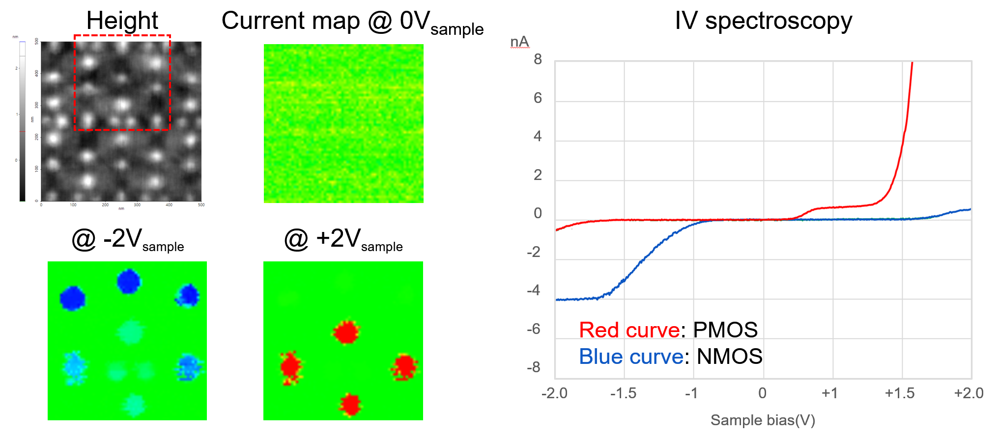
SRAM device arrays exhibit bias-dependent current behavior, where PMOS/NMOS regions and localized defective or leakage contacts show distinct electrical responses.
Conductive AFM IV mapping records a full I–V curve at every pixel, enabling pixel-level electrical imaging and rapid localization of defects without destructive sample preparation.
Scan Conditions
- System: FX40
- Scan Mode: IV Mapping
- Scan Size: 500 nm×500 nm, 300 nm×300 nm
- Scan Rate: 2 Hz
- Pixels: 256×256 for Imaging, 64×64 for IV Mapping
- Cantilever: AD2.8AS
(k=2.8 N/m, f=75 kHz)
- Sample Bias: -2 V – +2 V
×