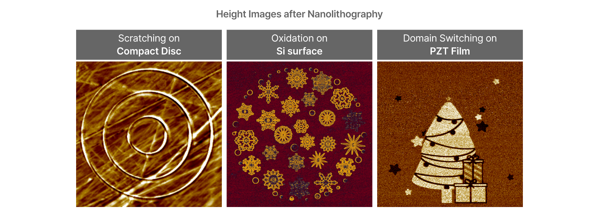
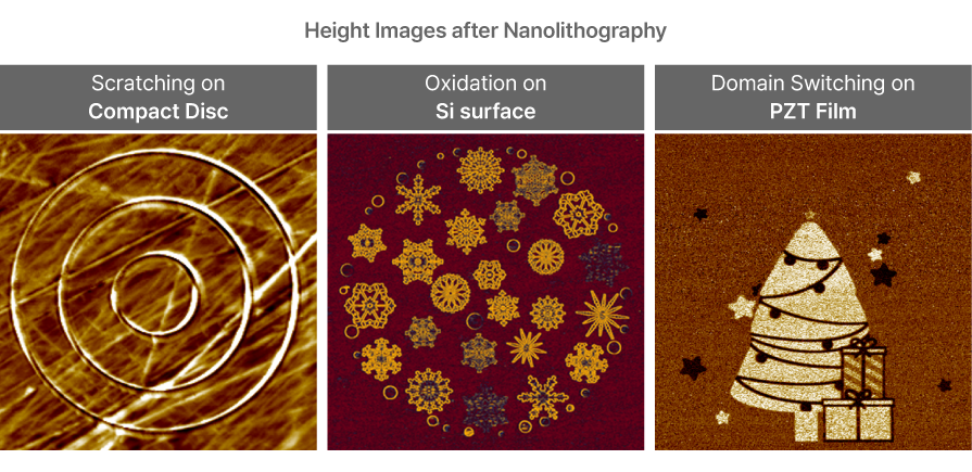
Lithography measures and modifies material surfaces by applying high force or voltage via the tip to etch, deposit, or pattern features at the nanoscale.
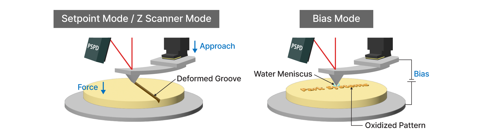
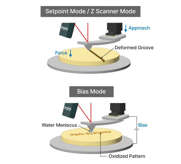
It operates primarily via two mechanisms: bias mode lithography, where an electric field generated by a voltage bias on the AFM tip induces localized chemical modification (such as anodic oxidation) to form nanoscale oxide features on semiconductor or metal surfaces, and force (Setpoint/Z scanner) mode lithography, which uses mechanical motion of the tip under controlled force to physically remove material or deform soft substrates. The process allows for the direct writing of arbitrary patterns with nanometer precision, without the need for masks or resist layers, and enables simultaneous characterization of surface topography and friction using modes like LFM or TFM. AFM nanolithography is particularly advantageous for fabricating prototype nanodevices, testing material properties, and producing features in environments unsuitable for electron beam or ion beam techniques, such as those requiring low energy input or ambient conditions.
Reasons to Use This Mode
The main advantage of nanolithography is its flexibility across various materials (metals, polymers, semiconductors) and its direct patterning capability without the need for complex masks or high vacuum with nanometer scale. This makes it an indispensable tool for fabricating novel nanodevices, creating templates for self-assembly, and studying fundamental surface phenomena.
Applications and Use Cases
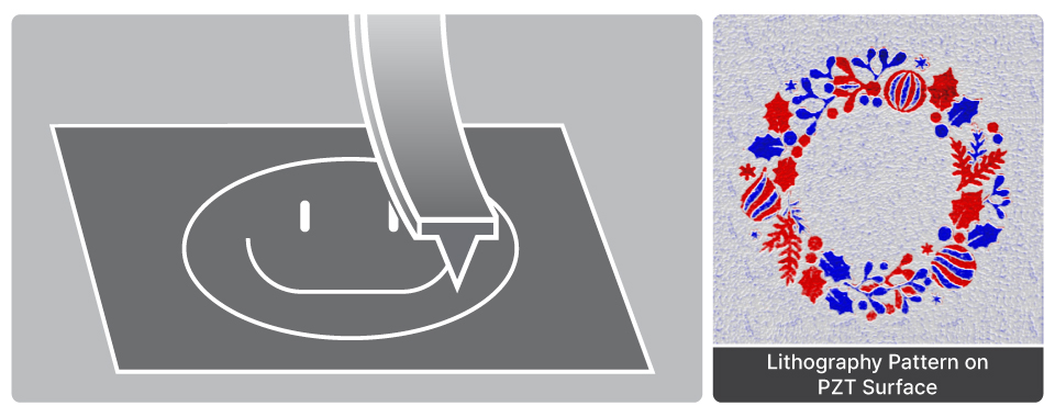
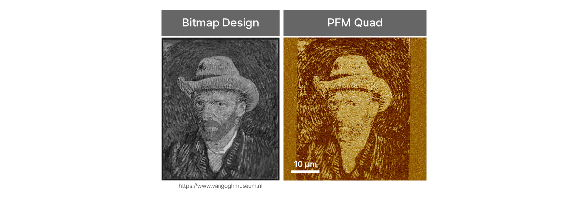
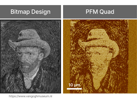
The images indicates AFM nanolithography applied to create a Vincent van Gogh image on a PZT surface by reorganizing ferroelectric domain orientation via tip bias. Using a bitmap design and controlled voltage, localized domain writing was achieved with nanometer precision, highlighting the technique’s capability to fabricate complex functional patterns for data storage, sensors, and advanced materials engineering.
Sample: PZT Surface
System: NX20
Scan Size: 50 µm × 50 µm
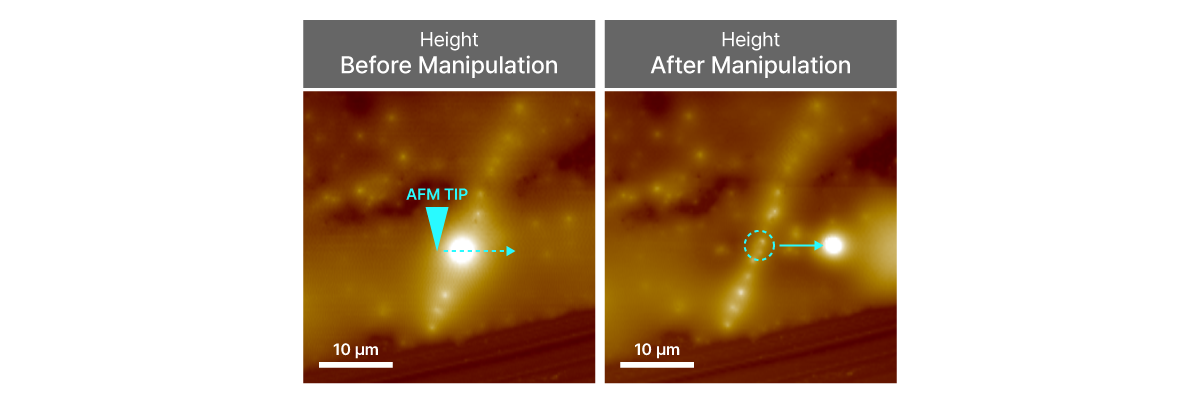
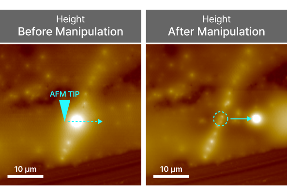
Here comes nanolithography by mechanical manipulation at the nanoscale, specifically showing controlled displacement of a silicon carbide (SiC) particle. By applying targeted force with the AFM tip, the particle was successfully shifted laterally on the substrate. This technique highlights nanolithography's capability for precision positioning and assembly of individual nano-objects.