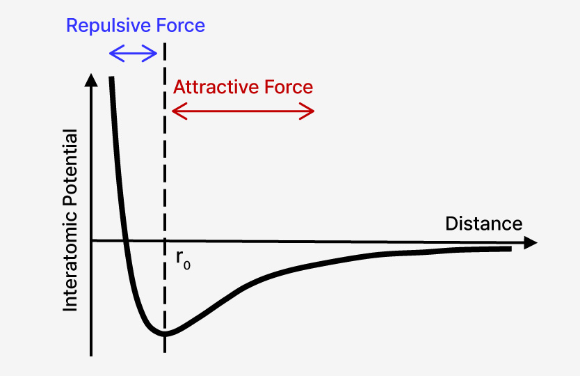
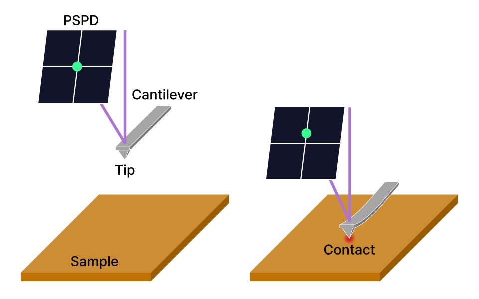
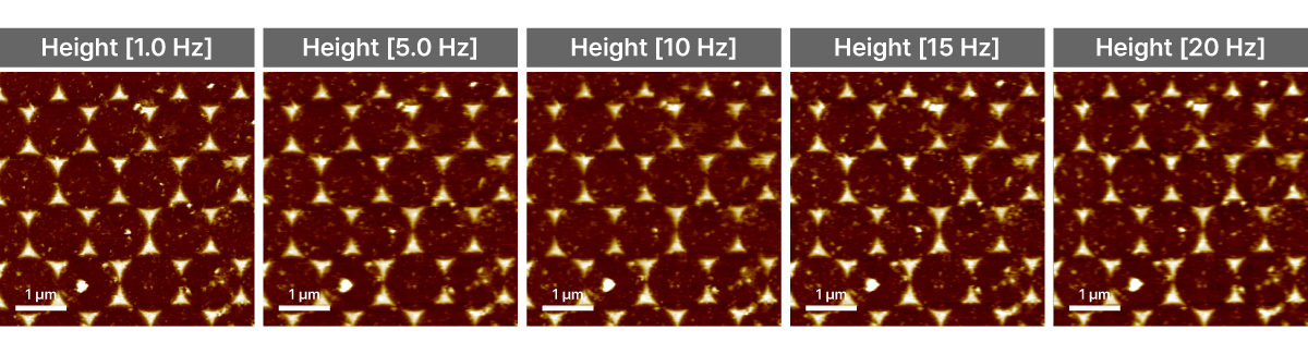
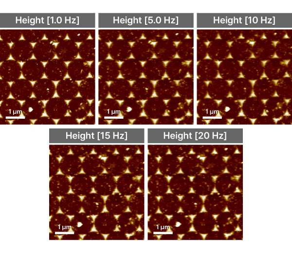
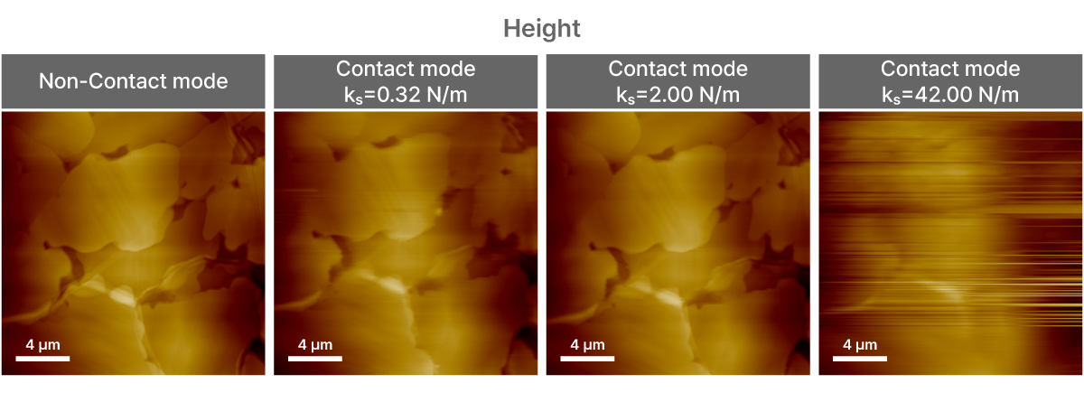
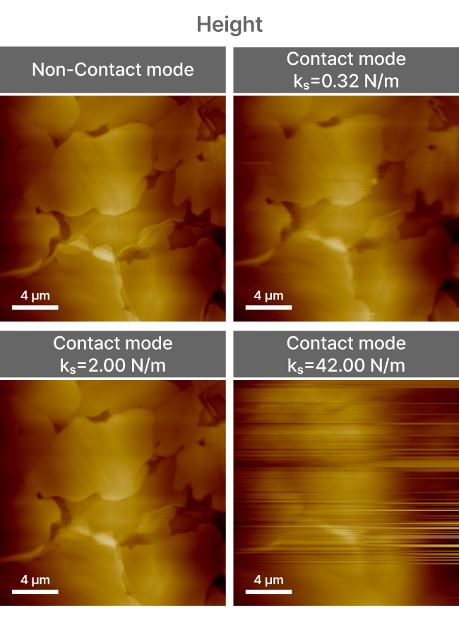
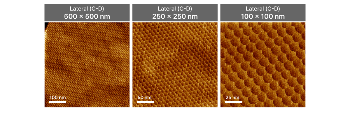
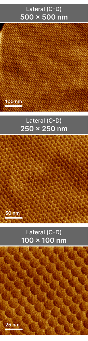
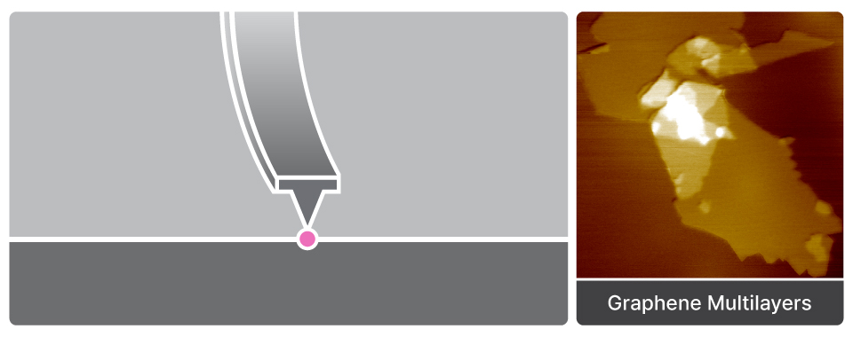
Contact Mode
High-sensitivity surface imaging through continuous contact between the AFM tip and sample, providing precise topographical information
What is Contact Mode
Contact Mode measures topography by detecting the repulsive force generated when the AFM tip remains in continuous contact with the sample surface, allowing high-sensitivity mapping of surface features through deflection of the cantilever. Contact mode serves as the base mode for various techniques that require physical contact between the tip and the sample, such as C-AFM, PFM, and SCM
Contact mode acquires surface topography by measuring the repulsive interaction between the AFM tip and the sample surface. When the tip–sample distance decreases below the equilibrium separation distance 𝑟₀, a steep rise in the interatomic potential induces a repulsive force, causing deflection of the cantilever in proportion to the force gradient.
In Contact mode, a laser beam is aligned onto the backside of the cantilever. Continuous mechanical contact between the AFM tip and the sample surface induces cantilever deflection as the tip follows surface contours. The resulting displacement of the reflected laser beam is precisely measured by the position-sensitive photodetector (PSPD) for real-time deflection monitoring. This signal is processed by the feedback control system, which regulates the Z scanner to maintain a constant cantilever deflection setpoint. This closed-loop control ensures stable tip–sample contact and enables high-fidelity mapping of surface topography at nanometer resolution.
Tip-sample contact induces cantilever deflection (bending), leading to a corresponding shift in the laser beam position on the PSPD.
Reasons to Use This Mode
Contact mode is the most straightforward and intuitive AFM scanning method, making it highly accessible and easy to understand. In this mode, the tip maintains continuous contact with the sample surface, enabling a fast and direct feedback response. This simplicity allows for rapid scanning and stable imaging across various samples, as illustrated in the images showing consistent pattern details from 1 Hz up to 20 Hz scan speeds.

Despite its ease of use, contact mode provides high-resolution topography, effectively capturing fine surface features. However, care must be taken when applying this mode to soft or delicate materials since the constant contact force can potentially cause surface damage. Nonetheless, its balance of speed, resolution, and simplicity makes contact mode a widely chosen technique for routine imaging and educational demonstrations, providing reliable and repeatable data across a broad range of experimental conditions.
  • Sample: AI Patterned Sample
  • System: FX40
  • Scan Size: 5 µm × 5 µm
Considerations in This Mode
In Contact mode, the selection of an appropriate AFM probe is critical to ensure measurement accuracy and sample integrity. A key parameter in AFM probe selection is the spring constant, 𝑘ₛ [N/m], which quantifies the cantilever’s deflection response to an applied force. This parameter directly influences the setpoint control and has a significant impact on both the precision of the measurement and the potential for sample damage.

When the cantilever’s spring constant substantially exceeds the sample’s stiffness, minimal cantilever deflection occurs, increasing the likelihood of sample surface damage due to insufficient force absorption. Conversely, if the spring constant is considerably lower than the sample stiffness, excessive cantilever bending compromises feedback stability, impairing the ability to maintain consistent imaging conditions during scanning.
  • Sample: Parafilm
  • System: NX10
  • Scan Size: 20 µm × 20 µm
Applications and Use Cases
Contact mode enables not only high-resolution surface topography mapping but also the detection of nanoscale patterns by utilizing lateral force signals that arise from frictional interactions between the tip and the sample. In particular, when applied to a graphene on hexagonal boron nitride (hBN) heterostructure, lateral force imaging allows for the precise visualization of moiré patterns, with clear periodic structures readily observed at scan sizes of 500 nm × 500 nm, 250 nm × 250 nm, and even 100 nm × 100 nm. This capability, which extends beyond conventional vertical deflection imaging, is especially valuable for distinguishing subtle features in 2D material systems and thin films.
  • Sample: Graphene on hBN
  • System: NX20
  • Scan Size: 500 nm × 500 nm, 250 nm × 250 nm, 100 nm × 100 nm