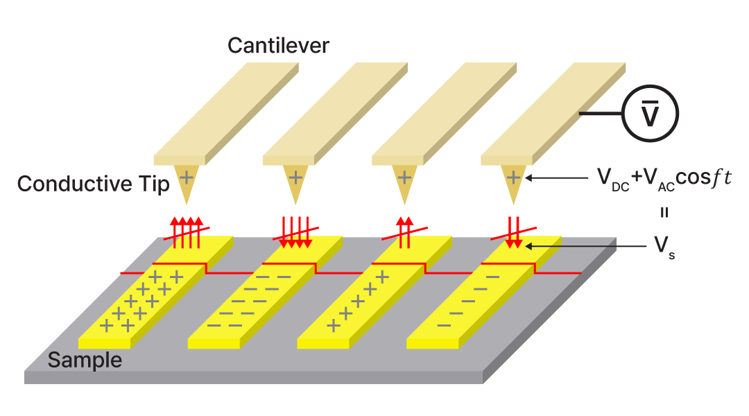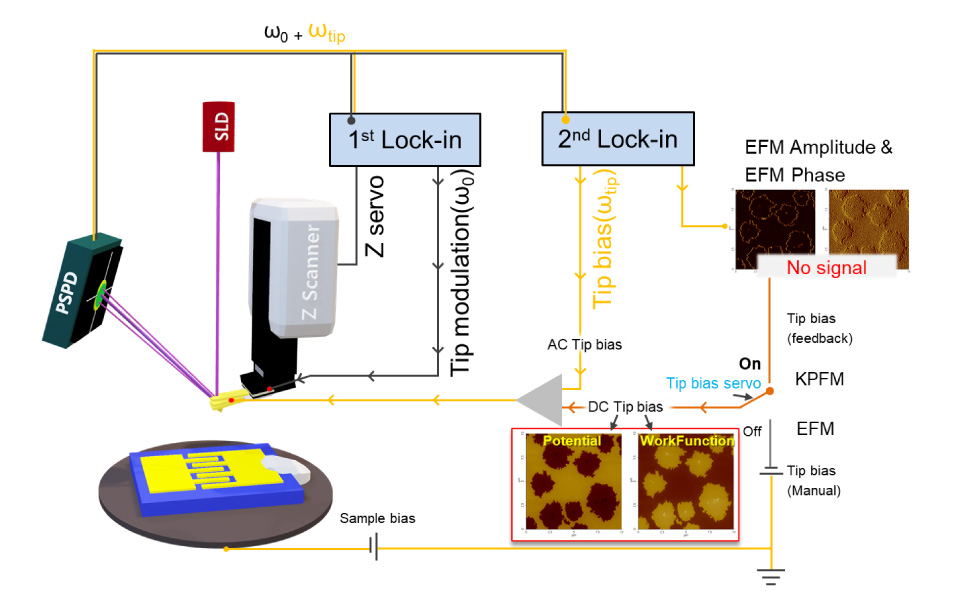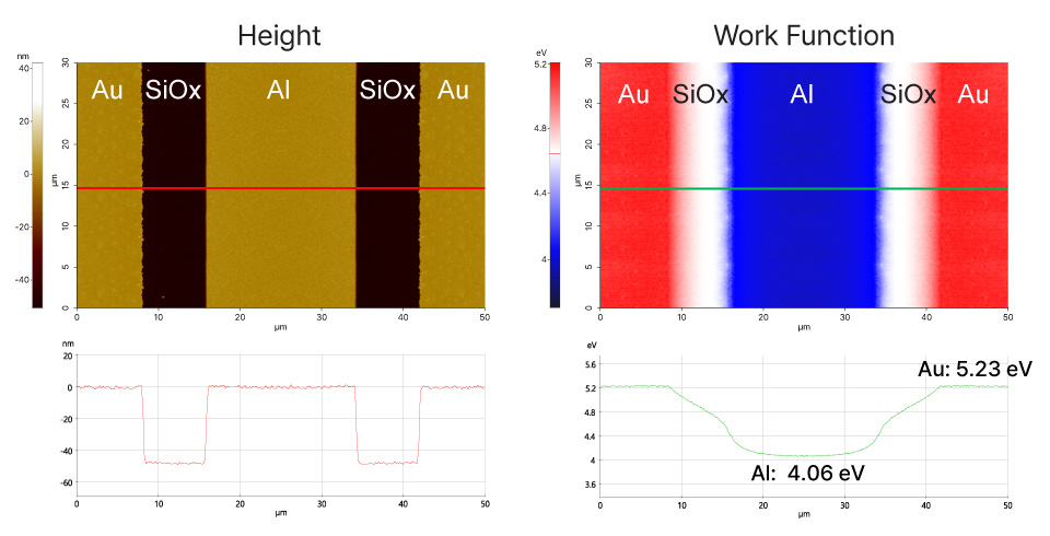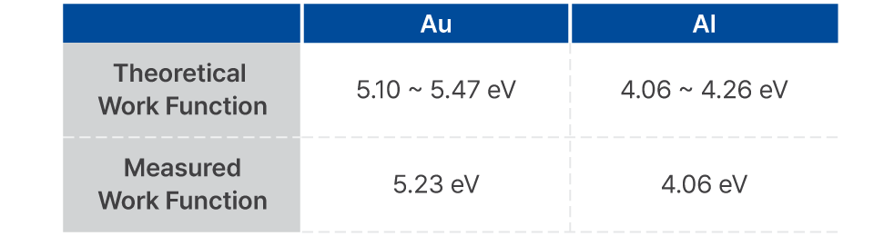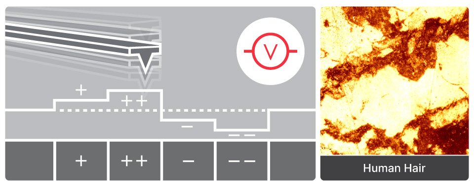
Kelvin Probe Force Microscopy
KPFM
Nanoscale imaging of surface potential and work function via electrostatic force compensation