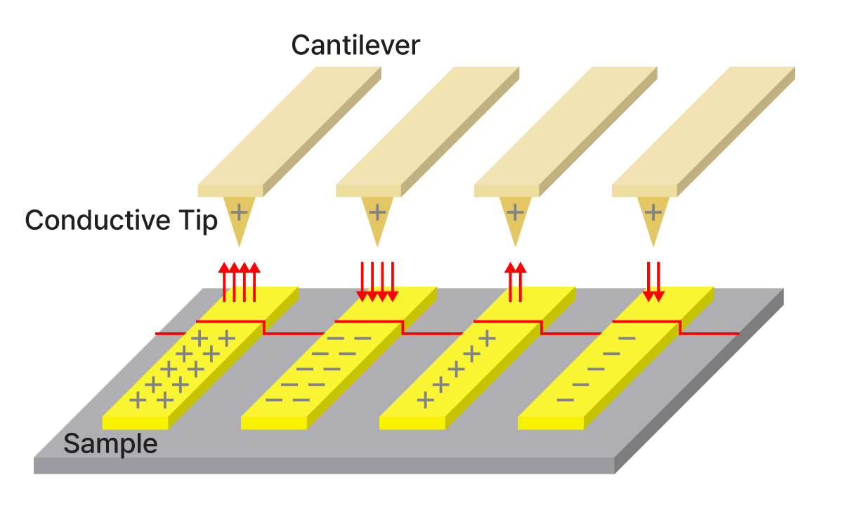
Electrostatic Force Microscopy
EFM
High-resolution mapping of surface electrostatic forces and potential variations by detecting long-range interactions between AFM tip and the sample surface