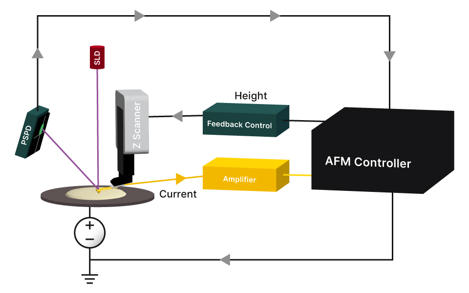
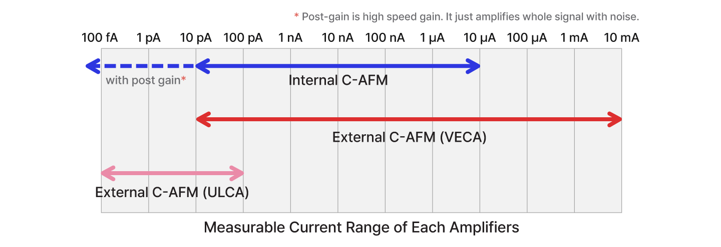
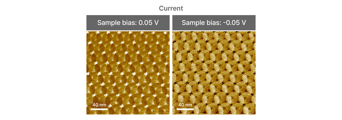
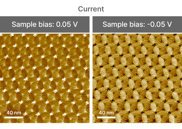
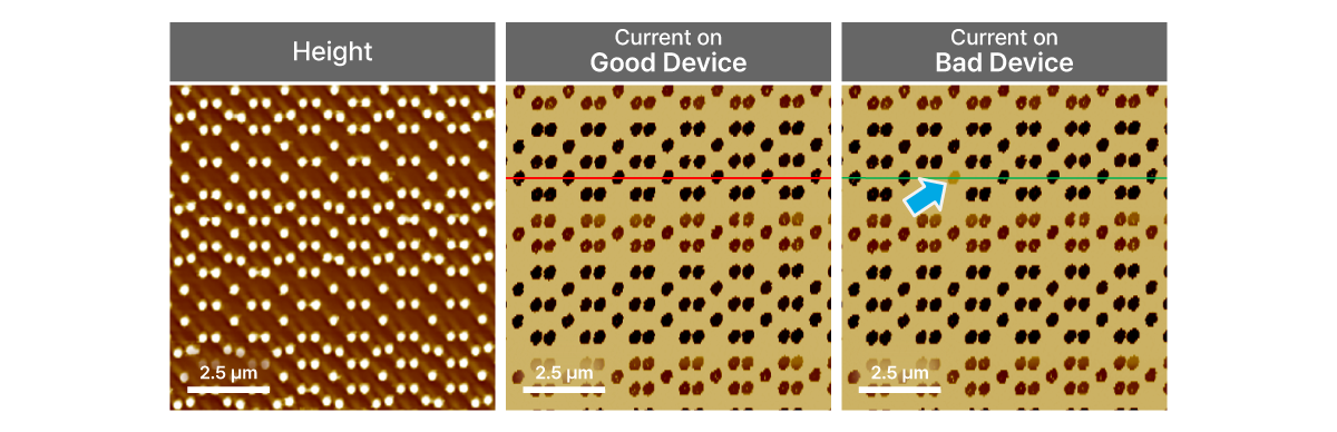
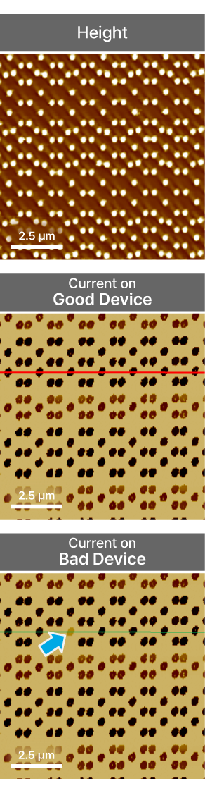
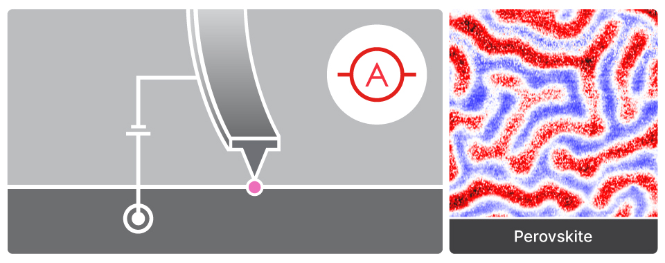
Conductive AFM
C-AFM
Mapping surface topography and local electrical conductivity via current flow through the conductive AFM tip in contact with the sample
What is C-AFM (Conductive AFM)
C-AFM measures both surface topography and local electrical conductivity by detecting current flow between the conductive AFM tip and the sample while maintaining continuous contact, enabling nanoscale correlation of structural and electrical properties. C-AFM enables local electrical characterization through IV spectroscopy, providing current–voltage responses at nanoscale contact points.
In C-AFM, a conductive tip, typically coated with platinum, gold, or diamond, scans the sample surface in Contact mode while a bias voltage is applied between the tip and sample. Maintaining constant mechanical contact, the tip simultaneously acquires topographic and local electrical data.

As it traverses the surface under a controlled load defined by cantilever deflection feedback, current generated through the nanoscale tip–sample junction is captured by a high-sensitivity current amplifier. The resulting signal is digitally mapped to visualize both current and surface morphology at nanometer resolution. By combining optical detection for topography with electronic detection for current, C-AFM enables clear correlation of structural and electrical characteristics, making it an essential technique for studying semiconductor devices, thin films, and 2D materials with localized charge transport phenomena.
Reasons to Use This Mode
Park Systems’ C-AFM offers three amplifier options: Internal C-AFM for standard current ranges, variable gain current amplifier (VECA) for high-speed measurements across a broad dynamic range, and ultra low current amplifier (ULCA) for ultra-low currents in sub-picoampere resolution. Proper amplifier selection—ULCA for high-resistance materials (0.1–100 pA), VECA for wide-range applications (pA to mA), and Internal C-AFM for general-purpose use—ensures measurement accuracy. For reliable data, careful sample electrical connecting, precise gain calibration, and environmental control are critical; ultra-sensitive experiments often require vacuum or inert environments to minimize noise and leakage
Applications and Use Cases
This application demonstrates how C-AFM provides exceptional spatial resolution for imaging nanoscale moiré superlattices that emerge in twisted bilayer graphene on hexagonal boron nitride (hBN). When these two materials are stacked with a controlled twist angle, their individual moiré patterns interact, creating a dual superlattice structure that can be either commensurate or incommensurate depending on lattice alignment. By performing current mapping at the nanometer scale, C-AFM reveals fine variations in local electronic conductivity that correspond directly to specific regions of the moiré pattern—showing aligned, ordered domains as well as disordered or mismatched areas. These differences in electronic properties are not readily distinguishable with conventional topographic AFM imaging alone. The capability to directly visualize complex, periodic structures and domain boundaries makes C-AFM a powerful tool for characterizing the electronic landscape of advanced 2D heterostructures, providing insights into domain size, stacking order, and twist-angle effects crucial for quantum materials research and device engineering.
  • Sample: Twisted Bilayer Graphene/hBN
  • System: FX200
  • Scan Size: 200 nm × 200 nm
C-AFM enables simultaneous acquisition of nanometer-scale topography and electrical current maps, facilitating precise identification of dopant distribution, leakage paths, and failure sites in semiconductor devices. In this example, current mapping was performed on both functional and defective SRAM devices under a -0.5 V sample bias, enabling direct comparison of electrical activity at the nanoscale. The C-AFM technique clearly revealed significantly reduced current at locations corresponding to defects, which were not distinguishable by topographical analysis alone. This method not only pinpoints regions of abnormal conductivity—including leakage paths and isolated failure sites—but also provides valuable quantitative data essential for detailed defect characterization and reliability assessment in advanced semiconductor manufacturing.
  • Sample: SRAM Device
  • System: NX10
  • Scan Size: 10 µm × 10 µm