
Click to see the original article on Worldfolio

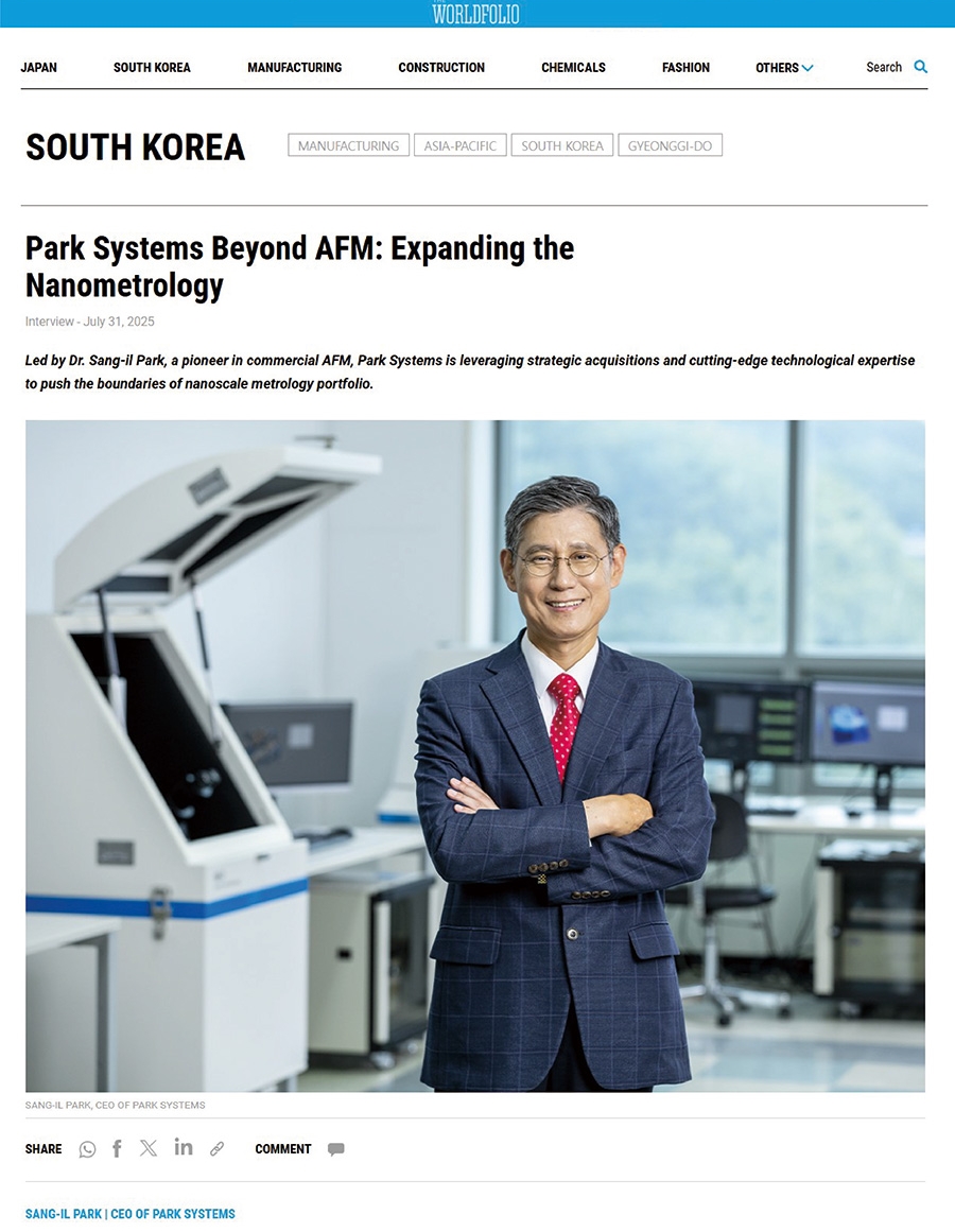
Led by Dr. Sang-il Park, a pioneer in commercial AFM, Park Systems is leveraging strategic acquisitions and cutting-edge technological expertise to push the boundaries of nanoscale metrology portfolio.
What are the challenges and opportunities for Korean suppliers within global supply chains?
I believe this is indeed a new opportunity for Korean SMEs. We are well-positioned to replace some of the roles that Chinese companies have been playing. There are many areas where we compete directly—such as steel, shipbuilding, automotive batteries, and semiconductors. In these overlapping industries, Korea can become a viable alternative to China for the Western market.
However, one major challenge is the language barrier. Large conglomerates can afford to have English-speaking personnel, but it’s far more difficult for SMEs to hire engineers who are fluent in English. While there are English speakers, most of them do not have an engineering background, which presents a real obstacle. This is a significant issue not only for Korean society in general but especially for Korean high-tech SMEs that aim to expand globally.
In my case, I was fortunate to study in the United States and to launch my first business in Silicon Valley. This gave me the ability to communicate fluently in English and to build a strong global network, which in turn enabled me to attract international talent. Unfortunately, most Korean companies lack this network, struggle with language barriers, and often don’t know how to make global connections. That’s a huge hurdle.
I also believe that Korea’s English education system is not functioning effectively and is in urgent need of reform. That’s just my personal observation.
That said, Korea is a unique country with incredibly talented, intelligent, and hard-working people. Once motivated, Koreans are capable of producing extraordinary results. This is how Korea’s industrial sectors became so successful. Take the automobile industry, for example. Twenty or thirty years ago, no one imagined Hyundai could become the world’s second-largest automaker. Samsung and LG were once chasing Sony—now they lead in the global TV market. With the right environment, motivation, and incentives, Korean companies can undoubtedly rise to the top of global markets. That’s my belief in the potential of the Korean economy.
In the semiconductor industry, Japanese and some European companies like ASML have traditionally dominated the materials and equipment sectors. However, during the trade conflict between Japan and Korea from 2018 to 2019, Korean firms proved their capacity for rapid localization. Companies like ENF Technology and Soulbrain swiftly captured domestic market share. After five or six years of solidifying their local dominance, do you believe these companies can now expand into international markets with ease?
I don’t believe it will be easy. These Korean materials and equipment manufacturers are fundamentally local companies. They tend to follow, not lead. To become truly global players, they must overcome significant language and cultural barriers, which they have yet to do.
Park Systems is a rare case where a Korean SME has become a global leader in its field, particularly in the AFM (Atomic Force Microscopy) market. What factors allowed your company to grow, expand, and lead globally—unlike many other Korean SMEs?
I’ve been involved in AFM from the very beginning. I founded the world’s first company to commercialize AFM technology. My education and business training in Silicon Valley were instrumental. I worked with Professor Calvin Quate at Stanford University, where the AFM was invented. This gave me early exposure to groundbreaking science and an unparalleled network of investors, lawyers, and mentors.
When I returned to Korea, I encountered a host of structural challenges—everything from company management culture to government regulations. For the first 10 to 15 years, growth was slower than I had hoped. But we eventually crossed the threshold and built a strong business platform and global brand recognition. Since then, our growth has accelerated significantly.
Park Systems is now a leading manufacturer of AFM systems and other nanoscale metrology instruments. We operate globally and are fundamentally different from most Korean companies of our size. We are a leader, not a follower. Many Korean firms manufacture versions of equipment originally developed in the U.S., Japan, or Europe, and sell them domestically at lower cost or with better service proximity. That model works locally but doesn't translate well overseas, where they lose their cost advantage and run into intellectual property issues. High-tech companies often battle fiercely over patents, and many Korean firms fear litigation.
We are different. We lead in technology. We hold a stronger patent portfolio and maintain a robust global sales network. Because of this, we aren’t afraid to operate internationally. In fact, it’s where we thrive.
AFM was invented in 1985 at Stanford University, in the lab of Professor Calvin Quate. I was a graduate student at the time, and after earning my Ph.D., I saw an opportunity to commercialize this revolutionary technology. In 1988, I founded my first company in Sunnyvale, California—the heart of Silicon Valley. We were the first to introduce a commercial AFM system to the market in 1990. At the time, we were also the sole supplier of AFM probes, which are the critical components of the technology. Even our competitors had to purchase probes from us. I was generous enough to supply them.
After spending 15 years in the U.S., I decided to return to Korea to begin the second chapter of my life. I sold my first company to Thermo Spectra in 1997, which was later acquired by Veeco Instruments. Interestingly, that first company eventually became part of what is now our biggest competitor.
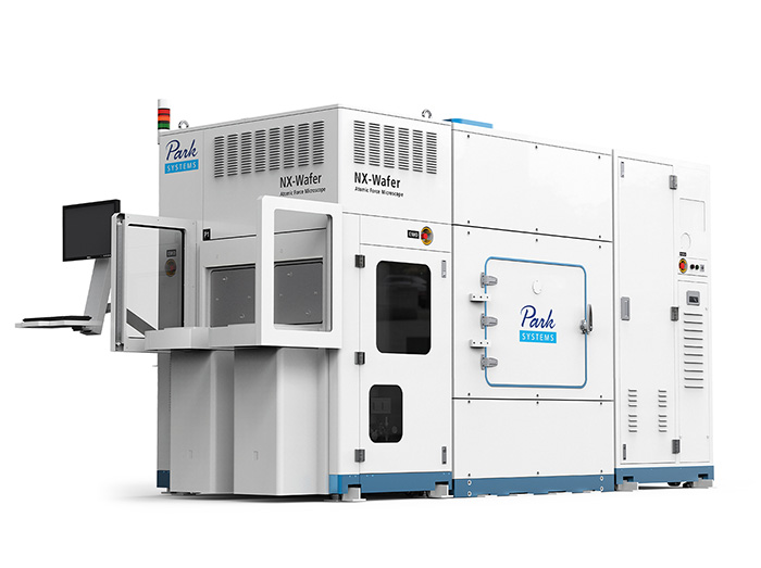
Later in 1997, I founded Park Systems—initially called PSIA. We rebranded on our 10th anniversary and went public in 2015. It took us 18 years to reach the IPO milestone, which was a long journey, but since then our growth has accelerated significantly. Today, our annual revenue stands at approximately $150 million. We employ around 550 full-time staff worldwide, and our market capitalization has reached about $1 billion. Our stock price rose from KRW 9,000 to KRW 200,000, making our investors very happy.
When you look at the growth curves among AFM manufacturers, ours is the steepest. In 2022, our revenue surpassed that of Bruker, which had long been the market share leader. We are now firmly in the number one position, followed by Bruker and Oxford Instruments.
Our success comes down to continuous and meticulous innovation. We transformed the core architecture of AFM by using a decoupled flexure scanner system that provides highly orthogonal scanning. We also developed the 3D AFM, Tip Scanning Head and pioneered True Non-Contact Mode AFM. This is a significant breakthrough—our True Non-Contact Mode remains unmatched. It’s very difficult to replicate and nobody else has managed to do it reliably. Most competitors use tapping mode, which causes tip wear and can damage the sample. Our True Non-Contact Mode avoids these issues, maintaining tip sharpness across hundreds of scans.
We also developed additional modes like PinPoint Nanomechanical Mode and Narrow Trench Mode, and have invested heavily in automating AFM. Traditionally, AFM required a highly skilled operator with a year or two of training. But our systems are so user-friendly now that even someone with just five minutes of instruction can generate an image. We’re also integrating hybrid solutions with White Light Interferometry(WLI), Imaging Spectroscopic Ellipsometry (ISE), and AFM-IR mode.
The basic principle of AFM involves using a sharp probe tip mounted on the end of a flexible cantilever. This is manufactured using MEMS (Micro-Electro-Mechanical Systems) processes. The probe is brought very close to the sample surface so that the atoms at the end of the tip can interact with the atoms on the surface. These atomic interactions—whether attractive or repulsive—allow us to measure forces at the nanoscale.
When the tip approaches without touching, the atoms attract each other. If the tip comes into contact, the interaction becomes repulsive. These tiny forces are detected by the deflection of the cantilever, which oscillates near its resonant frequency. A laser beam is focused on the top of the cantilever, and as the cantilever moves—due to surface interaction—the angle of reflection changes. By analyzing this deflection, we can determine the topography of the surface. We then scan across the X and Y axes while maintaining feedback in the Z-axis to create a height map of the sample.
Traditional AFMs use tube scanners, which are simpler and less expensive but introduce serious measurement limitations. When scanning in X and Y, these tube systems also affect the Z movement, creating crosstalk, background curvature, and reduced accuracy.
We solved this by redesigning the scanner system with decoupled flexure scanners. The XY scanner moves only the sample in the horizontal plane, while a separate one-dimensional flexure scanner moves the probe vertically. This separation allows for highly accurate measurements, free from cross-axis interference.
Another key breakthrough was our development of the True Non-Contact Mode. In this mode, the tip stays within the attractive force region, never entering the repulsive zone. This is different from tapping mode, which is more common because it is easier to implement—but it wears out the tip and can damage or contaminate the sample. In contrast, our True Non-Contact Mode preserves the tip's shape. The tip diameter remains consistent—around 5 nanometers—even after 100 to 200 scans. In tapping mode, the tip quickly becomes blunt.
In your seminars, you often show data from 15,000 repeated measurements. Is there ever a point at which the tip still becomes blunt?
Not if you stay strictly within the attractive Van der Waals interaction region. As long as you maintain that condition, there’s no tip wear. It can essentially last indefinitely. Of course, if the tip accidentally enters the tapping region—due to environmental changes or other variables—then wear can occur. But under controlled conditions, the probes used by Park Systems’ True Non-Contact Mode™ are far more durable than those by conventional modes.
You’ve also automated the oscillation frequency and optimized scanning parameters. Can you elaborate on how you maintain such high precision during scanning?
We meticulously optimize operational parameters, including frequency and oscillation amplitude. Most importantly, our Z-servo system must respond extremely quickly to any surface variation. If the surface height changes and the Z-servo is too slow, the tip may crash or enter tapping mode. So we’ve significantly enhanced our Z-servo performance—both mechanically and through sophisticated software and control algorithms.
Theoretically, what you describe seems simple. Why haven’t your competitors been able to replicate this in practice?
They haven’t invested the necessary time. In theory, any skilled engineer could develop a True Non-Contact Mode if they focused on it for two to three years. But most of our competitors have spent decades promoting their tapping mode as the best. For them to suddenly shift and claim non-contact mode is superior would essentially validate our approach. It creates a marketing dilemma for them.
Even if they do manage to build a non-contact mode, ours would likely still be better. We’ve accumulated years of fine-tuning and experience. In this field, that depth of refinement makes all the difference. That’s why they continue to emphasize tapping mode, even though it has clear limitations—like tip wear and sample damage, especially when measuring soft surfaces or in the presence of thin liquid layers.
That said, if a customer specifically requires tapping mode for hard surface measurement, we can certainly support that as well. We offer both.
A major driver of our growth has been the increasing demand in markets like semiconductors, advanced packaging, EUV photomasks, and display manufacturing. These industries face persistent challenges in measuring increasingly small structures with traditional tools. They are constantly searching for better metrology solutions, and this is where our AFM systems truly shine.
Especially in semiconductor applications, AFM offers a remarkably wide range of capabilities. People often ask, “What exactly can your AFM measure in the semiconductor process?” The answer is almost everything—from front-end to back-end processes. Our systems can measure surface roughness, height, depth, width, angle, perform CMP metrology, wafer edge metrology, defect review, and even electrical conductivity. The list goes on. As back-end processes become more complex, compact height measurement and redistribution layer metrology have grown increasingly important. We’re also contributing in the EUV mask segment, not just for defect review but even for repair.
We’ve worked closely with partners like IMEC, with whom we’ve had multiple joint development projects. These collaborations served as a stepping stone, establishing Park Systems as a trusted name in the semiconductor industry. Once we gained that credibility, customers started asking, “Can you measure this? Can you build that?” That was the moment we realized we could expand beyond AFM.
One of our first major expansions was through the acquisition of Accurion, a world leader in imaging spectroscopic ellipsometry (ISE) and active vibration isolation (AVI) systems—both of which are highly complementary to our AFM business. We are now developing an industrial version of their imaging spectroscopic ellipsometry (ISE), which is already being used in R&D labs. The prototypes are ready, and we’re working closely with customers to validate their performance and secure budgets. We hope to generate our first revenue from industrial ISE this year.
More recently, we acquired Lyncée Tec, pioneers of digital holographic microscopy (DHM) based in Switzerland. We believe their DHM platform holds significant promise for advanced packaging applications, particularly where speed and throughput are essential. DHM can instantly capture absolute 3D topography in milliseconds, making it highly suitable for high-volume manufacturing metrology.
You mentioned that you're developing industrial platforms for both Lyncée Tec and Accurion. What is your expected timeline for the commercialization of these systems?
We’re pushing to get them to market as quickly as possible. We're already measuring customer samples using research versions of these tools. For ISE, we have prototypes ready and are working through the customer validation process. It takes time to convince clients, secure their budgets, and complete the procurement cycle. But our goal is to begin generating revenue from industrial ISE within the year.
What semiconductor processes or inspection goals will ISE focus on?
ISE is particularly effective for thin-film characterization and optical critical dimension (OCD) measurements. Traditional spot ellipsometry has limitations—the spot size is typically 20–30 micrometers and can’t be much smaller. That means the sample needs to have a uniform area large enough for the spot, which introduces potential errors if there’s a boundary or feature nearby.
Our imaging ellipsometry, on the other hand, illuminates the surface uniformly and collects the reflected signal using a 2D camera array. It generates hundreds of thousands of spectral data points in parallel, allowing the user to select any point of interest for detailed ellipsometric analysis. While this isn’t imaging in the conventional sense—like a microscope—it still gives you a “map” that enables far more precise measurement selection. It's a game-changer for thin-film uniformity and OCD analysis.
Is this a combination of ISE and AFM? Are they integrated systems, or do they operate separately?
They are separate systems, but closely related. AFM focuses on nanoscale surface metrology—step heights, roughness, angles—while imaging spectroscopic ellipsometry is highly effective for thin film characterization and uniformity analysis. Traditional ellipsometry provides only one data point per measurement, but our imaging system delivers thousands—potentially hundreds of thousands—of data points at once. This allows customers to map film variations across the entire wafer. It’s an incredibly powerful complement to AFM.
With Accurion, we already had a robust ellipsometry technology and industrial platform. What we’ve done is replace the AFM module with the ISE module on our inline system. We’re now actively engaging with customers to explore applications. One promising use case is defect inspection—not in the traditional sense, but for detecting process-induced thickness variations after CMP. These types of “Z-defects” can be easily missed by conventional inspection tools. ISE can catch them.
That said, AFM remains our core product and primary revenue driver. We offer both research and industrial AFMs. But now, with holographic microscopy and imaging ellipsometry in our portfolio, we’re integrating these into our inline metrology platform—pushing toward broader applications in high-volume semiconductor manufacturing.
As a global company, our headquarters is based in Suwon, Korea, but we have a strong international footprint. We operate direct subsidiaries in Japan, China, Taiwan, Singapore, India, Germany, the UK, France, as well as Accurion's office in Göttingen and Lyncée Tec’s office in Lausanne. In the U.S., our headquarters is in Santa Clara, with additional offices in Boston and Mexico City.
We also invest in academic outreach and knowledge sharing. Since 2014, we’ve hosted regional NANOscientific Symposium—academic events that bring together leading researchers and customers. Last year, we held events in Bangkok, Tokyo, Suzhou, Munich, Arizona, and Busan. We also publish the NANOscientific Magazine, which emerged from our earlier newsletter efforts. Newsletters often get discarded quickly, but a magazine has lasting value. Through it, we share stories, interviews with customers, and even insights from global leaders like the White House Science and Technology Advisor. We believe these initiatives help build trust and community in our field.
We’ve already become a strong and globally recognized company. I’ve achieved my initial goal: to build the world’s number one AFM company with over $100 million in revenue and a market capitalization exceeding $1 billion. But now, we’re setting our sights even higher—to become a global top-tier player. Some of the industry leaders we look to, like KLA, have a market cap of $100 billion and annual revenues of $10 billion. Of course, these companies were established decades—sometimes over a century—ago. Carl Zeiss, for example, has a long history. But we’re now taking deliberate steps to follow that path.
One of the most important steps is strengthening our top leadership. We’re recruiting world-class executives and board members. This year alone, we brought on two highly respected figures. Dr. Hee Gook Lee, the former CEO of LG Electronics, is now advising us after his retirement. We also welcomed Professor Kiyoung Choi, a former Minister of Science and Technology and longtime professor at Seoul National University. These are influential leaders who understand both the industry and national science policy, and they are deeply committed to our mission.
In addition to our acquisitions of Accurion and Lyncée Tec, we’re actively negotiating with over five other companies—domestic, European, and American. We’re expanding both our product portfolio and our geographical reach. These strategic moves are not just about growth—they are about building a robust, future-ready technology ecosystem.
We’re also making targeted investments in key technologies. One example is our partnership with Kim’s Reference founded by Dr. Kim from KRISS—the Korea Research Institute of Standards and Science. It’s Korea’s equivalent of NIST. Dr. Kim is a global authority in standard sample calibration for film thickness and linewidth. We’ve invested in his efforts to develop highly precise samples, which we now use in our own metrology tools.
Another investment was made through a German company named Lightsource.tech for semiconductor inspection. Metrology tools require extremely bright and broadband light for fast, noise-free measurements and effective spectroscopy. A powerful light source is essential for accuracy and throughput, and this partnership will help advance that capability.
Linear motor technology is another area we’re monitoring closely. While it’s a well-established technology, there's room for improvement in speed and stability—both critical for modern sample movement. We’re currently evaluating candidates to join us in developing or sourcing these components.
At the same time, we’re deepening collaborations with global academic leaders. We’re working with Professor Nakajima at the Tokyo Institute of Technology on dynamic mechanical analysis; Professor John Sader at Caltech on cantilever spring contact; Professor David Goldhaber-Gordon at Stanford University on torsional force microscopy; and most recently, we signed an agreement with Professor Eric Ma at UC Berkeley on scanning microwave impedance microscopy. Here in Korea, we’re also collaborating with Professor Kyung Woo Lee at Seoul National University, a world expert in deep image restoration.
This area—AI-based image restoration—is becoming increasingly important. It’s especially critical in digital holographic microscopy, where image quality depends on mathematical modeling and signal reconstruction. Artifacts and noise are a challenge, and AI can help us recover the original image more accurately. While AFM delivers more direct measurements, DHM requires complex interpretation, and that’s where our AI partnerships bring value.
Once we develop a new technology, we make it a priority to protect it. Our intellectual property strategy is a core part of our competitiveness. We’ve partnered with top law firms in Silicon Valley, including IP strategist Stanley Chang, who helps us craft stronger patent claims and ensures our filings are enforceable. We also work with Natalie Huh from Quinn Emanuel, the world’s largest litigation firm. It’s not just about protecting our own technology—we also have to defend against infringement claims. We've already received letters from attorneys in the U.S. alleging that we were infringing on their patents. We responded forcefully, and they backed down. Our IP position is strong, and we intend to keep it that way.
We’re also investing in our people and facilities. Our new global headquarters is under construction in Gwacheon City. The structure will be completed this summer, and we plan to move in by early next year. We believe that a well-designed, inspiring workspace will boost morale, help attract top talent, and reinforce our team’s pride in what we’re building together.
Recently, we received coverage from a global financial analyst for the first time. Korean analysts have followed us for years, but global analyst coverage is a rare milestone for a mid-sized Korean company. We already have a strong base of foreign investors—about one-third of our shares are held by them—and I personally engage with investors through meetings and video conferences with stakeholders in New York, London, and Singapore. Investor relations are built on trust, and we work hard to maintain those relationships. They don’t want to throw money at a company they don’t know. We make sure they understand who we are, what we’ve achieved, and where we’re going.
Over time, I’ve come to believe that our greatest asset is not just our technology or our engineering talent—it’s our corporate culture. In the past, I would have pointed to our AFM innovation or technical expertise as our most valuable strength. But now I believe our culture—based on mutual respect, trust, and autonomy—is what truly sets us apart. Our people enjoy working here. They invite their friends to join us. That organic growth, fueled by internal satisfaction, is attracting talent, investors, partners, and loyal customers. It creates a snowball effect: as we succeed, we can treat our people better, which in turn drives even greater success.
This is the essence of a free market economy. While it’s true that “the rich get richer,” that’s not our ultimate goal. Personally, I have more than enough for my own needs. I believe our higher purpose is to create maximum value for others—to make people happier. We’re all part of an interconnected society, and life has meaning when our work is recognized by others as valuable. We must always think about how we’re serving our customers, colleagues, suppliers, shareholders, and society at large. Our goal is to make a positive impact.
You also mentioned the application of AFM in photomask defect detection. Could you elaborate?
AFM is excellent for imaging photomask defects. Traditional tools can generate defect maps, but they don’t offer the resolution or shape information AFM provides. For instance, SEM can show contrast, but it can’t determine whether a defect is a bump or a pit. AFM gives that topographical insight. In fact, it can even repair defects. We've demonstrated cases where a protruding particle was identified and then physically brushed away using an AFM probe. In another case, a bridge defect—where two structures were mistakenly connected—was cut using a diamond AFM tip, restoring the intended separation.
How do you return to the same location with precision after changing the tip?
That’s part of our proprietary technology. We’ve developed high-precision stages and automated tip exchange systems. Optical vision assists with navigation, and we calibrate for thermal drift and mechanical error. On a 300mm wafer, finding the same micrometer-sized feature with nanometer accuracy is like locating a 1-meter boat in the Pacific Ocean. But we’ve built systems that can do just that.
With major players like Intel investing heavily in EUV production, will that sector become a major revenue driver for Park Systems?
EUV is an important segment, but it won’t single-handedly drive dramatic revenue growth. It will complement our broader portfolio. AFM is a general-purpose diagnostic tool. Initially, customers used it for various measurements—CMP, defect review, trench depth, roughness, angle, and more. We realized that AFM was becoming a reference tool for the entire process. As customers adopted it in one area, they began integrating it into additional steps, leading to recurring demand. Optical and SEM tools often require calibration, and AFM provides the gold-standard measurement. That’s how we’re growing.
You mentioned a recent cultural shift at Park Systems. How would you like your customers to view the company today? Do you have a slogan for 2025?
“The Best Nanoscale Metrology Solutions Partner.” That’s how we want to be known. For example, a Taiwanese customer had difficulty measuring redistribution layers using optical tools. They asked for our help. We used white light interferometry and creative scanning methods to identify the correct measurement approach. It wasn’t easy—we struggled for six months—but eventually delivered a solution they were thrilled with. They bought five systems. That’s what defines us: we respond in real time, invent on the fly, and deliver solutions that didn’t previously exist.
Other companies—from the U.S., Korea, and beyond—come to us with challenges. Our engineers, our academic partnerships, our speed, and our cost advantage—especially compared to U.S. and European firms—allow us to deliver meaningful results.
If we return a few years from now to celebrate an anniversary with you, what would you hope to have achieved by then?
I hope we’ll continue growing—in revenue, in customer base, in reputation, and in our people’s pride. One of my greatest joys is that our employees genuinely respect and appreciate me. That’s rare for a CEO. In many companies, employees grumble about management. But at Park Systems, the culture is different. I take great pride in that.
Of course, the larger we become, the harder it is to maintain rapid growth. It’s easy to grow from $10 million to $15 million. But scaling from $100 million to $150 million—or beyond—is far more difficult. Still, my dream is to grow to $1 billion and ultimately become a global top-tier player. That’s the vision I’m committed to.