Introduction
Graphene, a single layer of carbon atoms arranged in a two-dimensional lattice, has attracted significant attention due to its exceptional electrical, thermal, and mechanical properties1-3. Its potential applications range from nanoelectronics to sensors, catalysis, and energy storage. However, precise manipulation and patterning of graphene at the nanoscale remain challenging, hindering the utilization of its unique characteristics in practical applications. Atomic Force Microscopy (AFM)-based nanolithography has emerged as an effective method for nanoscale fabrication4,5. AFM-based nanolithography enables the direct writing of patterns on a material's surface with nanometer precision. This technique employs a sharp AFM tip to induce local modifications to the material, facilitating the creation of intricate patterns on graphene layers6 (Figure 1). The cutting process involves a careful
balance of various parameters, including tip bias, AFM tip applied force and approach speed, and environment conditions, to achieve optimal results. Optimization of these parameters is essential for effectively cutting graphene and generating well-defined nanopatterns.
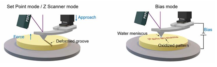
Figure 1. AFM-based nanolithography. Set Point / Z Scanner mode: The AFM system exerts a significant force to mechanically deform the sample surface by scratching it. Bias mode: AFM tip bias is applied on the patterned area to create an oxidation layer (height~ 1-2 nm) on a bare surface.
In this study, we conducted a feasibility test to optimize AFM-based nanolithography parameters to achieve precise nanopatterning on a single layer of graphene (Figure 2). Through a series of trials, we systematically investigated the influence of key
variables on the cutting quality and resolution of nanometer-scale lines. By enhancing the understanding of AFM-based nanolithography techniques, we aim to contribute to the advancement of graphene applications across various fields, particularly in the development of next-generation nanodevices.
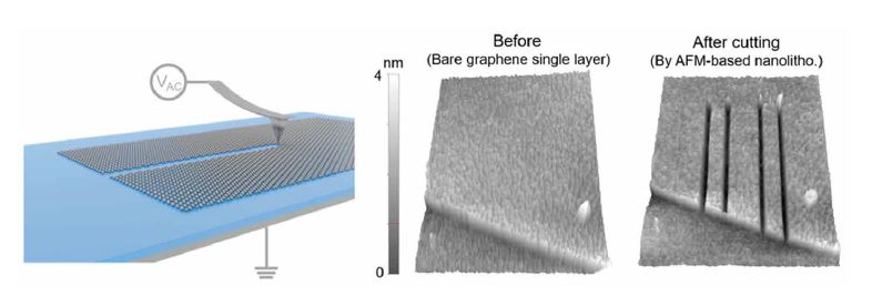
Figure 2. Thin layer graphene cutting by AFM-based nanolithography.
Materials and Methods
Thin graphene layers on a silicon (Si) wafer were prepared to evaluate the cutting or patterning of graphene layer by AFM-based nanolithography.
For AFM-based nanolithography, a commercial AFM system, NX10 (Park Systems), was used7. The AFM system and probe were calibrated prior to experiments to ensure accuracy. The two detailed modes of AFM-based nanolithography used in this study are described as follows.
1.Set Point / Z Scanner mode (Mechanical method): In mechanical AFM lithography, the AFM tip applies a controlled, high force to physically etch or “cut” through the graphene layer. By tracing a predefined pattern, the tip can cut specific
shapes or pathways into the graphene with nanometer precision.
2. Bias mode (Electrochemical method): In this mode, a bias voltage is applied between the AFM tip and the substrate, creating an electric field that induces a local oxidation reaction at the graphene surface. This results in oxidized graphene
regions that can be selectively removed, effectively "cutting" the graphene. It is especially useful for precise and controlled modifications of graphene without requiring high physical force.
Investigation of graphene cutting quality under varying parameters
The mechanical cutting method in AFM-based nanolithography is straightforward8. It cuts the graphene layer by precisely controlling the force applied to it and can be performed under ambient conditions, making it more accessible than methods
requiring vacuum or controlled environments. However, this method has some notable drawbacks. The AFM tip is prone to wear and damage due to high force applied during cutting, which can reduce accuracy over time and necessitate more frequent tip replacements. As shown in Figure 3, there is also a risk of unintended damage or deformation to the surrounding graphene due to the mechanical force, which can degrade the quality of the patterned structure. This often results in rough or jagged edges along the cut regions—especially at higher forces—potentially impacting the electronic properties of graphene where smooth edges are
essential.
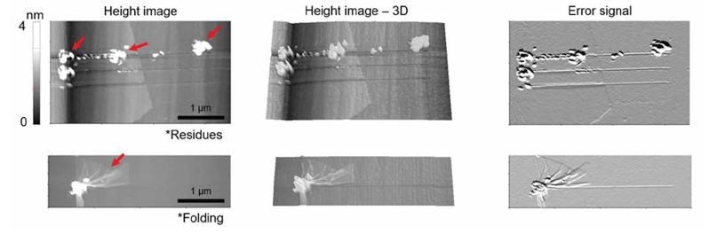
Figure 3. Mechanically graphene cutting by AFM-based nanolithography with Set Point mode. Lines were drawn with force after the AFM tip made contact to induce scratches on the surface.
An alternative method, Bias mode in AFM-based nanolithography, was also tested with various parameters. This method involves a bias voltage between the AFM tip and the substrate generates a localized electric field at the contact point or near-contact region with the graphene. This electric field causes water molecules from the ambient environment or intentionally introduced moisture to undergo electrolysis, producing reactive oxygen species like hydroxyl ions. These reactive oxygen species interact with the carbon atoms in graphene, leading to oxidation and transforming specific portions into graphene oxide, which has distinct electrical and
chemical properties from pristine graphene. The use of AC bias enhances this process by generating a periodically oscillating electric field, which prevents continuous charge buildup and reduces unwanted side reactions. This field enhances the formation of reactive oxygen species, enabling precise, localized cuts9,10.
We first demonstrated graphene cutting possibilities according to the applied bias. Consequently, the applied voltage significantly affected the extent and depth of the oxidation on graphene, which influences the degree of cutting (Figure 4).
1.No bias (0V): At low or zero voltage, oxidation is negligible due to an insufficient electric field to initiate the electrolysis of water molecules and generate reactive oxygen species. As a result, no significant cutting or oxidation occurs on the
graphene surface.
2. Low bias (3V): With moderate voltage, a controlled oxidation process begins. At this range, the electric field is sufficient to start generating reactive oxygen species, which then interact with the graphene surface to create shallow, localized
oxidized regions. These regions are often less deep and don’t fully "cut" through the graphene, making them more suitable for modifying surface properties or creating conductive paths without fully isolating sections of graphene.
3. High Bias (10V): At higher voltages, the oxidation process intensifies as the stronger electric field generates more reactive oxygen species and increases the rate of oxidation. This can lead to deeper oxidation that might extend through
the graphene layer, effectively "cutting" or isolating parts of it. At sufficiently high voltages, oxidation depth can be controlled to fully penetrate the graphene layer, creating distinct regions that are electrically separated from each other.
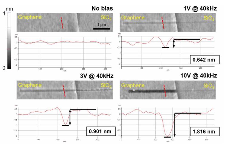
Figure 4. Electrically graphene cutting by AFM-based nanolithography with AC bias mode. At 1 and 3 V, the lines are thin and blurry; however, when 10 V is applied, the etching line is successfully formed with smooth edges and no residue.
Humidity is one of the most important factors for the success rate of graphene cutting via AFM-based nanolithography. The presence of ambient water molecules is critical, as they enable the generation of reacti ve oxygen species needed for oxidation11. In Figure 5, at 10% relative humidity, the water layer between graphene and the Si substrate is minimal or nearly absent, which limits reactive oxygen species production and leads to a very low success rate for cutting. Oxidation under these conditions is weak or incomplete, resulting in inconsistent outcomes. When humidity increases to 20–40%, the water layer is slightly thicker, providing more reactive oxygen species; however, the amount remains insufficient for deep or reliable oxidation, producing shallow or incomplete cuts and only a slight improvement in success rate.
At humidity levels above 60%, the water layer is well-established, offering ample water molecules for reactive oxygen species production. This level is confirmed to be optimal for the Bias mode of AFM-based nanolithography, as it enables a strong, stable oxidation reaction that results in deep, consistent cuts with high success and precision9.
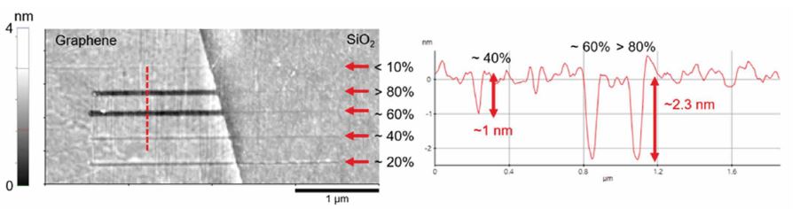
Figure 5. Graphene cutting quality according to humidity environment. A humid environment of 60% or more is recommended for accurate cutting.
The presence of a water layer between the graphene and the Si substrate can also influence the result in graphene cutting by AFM-based nanolithography. This water layer, which is present due to ambient humidity or adsorbed water molecules, plays an essential role in the anodic oxidation reaction by providing a medium for electrochemical processes. Figure 5 shows that water molecules are necessary to produce reactive oxygen species through electrolysis. The water layer between the graphene and the Si substrate can contribute additional water molecules, enhancing the local availability of reactive oxygen species at the oxidation site9.
Based on this theory, it is hypothesized that, given adequate time for a water bridge to form between the AFM tip and the sample surface, the directional dependence of the cutting process can be mitigated. Here, “adequate time” does not refer merely to a slow scan speed; rather, it involves a deliberate deceleration of the AFM tip immediately prior to contact with the sample, allowing sufficient time for the water bridge to establish itself between the AFM tip and the sample surface. As shown in Figure 6, when the AFM tip was allowed to contact the sample (graphene or Si substrate) very slowly, it was confirmed that the graphene was successfully cut in any direction. This is because when the AFM tip is very close to the graphene surface, a water bridge forms first, causing local oxidation and removing the graphene beneath it. SmartScanTM (Park Systems’ AFM operation software) enables precise control of these parameters, resulting in more consistent and effective graphene cutting.
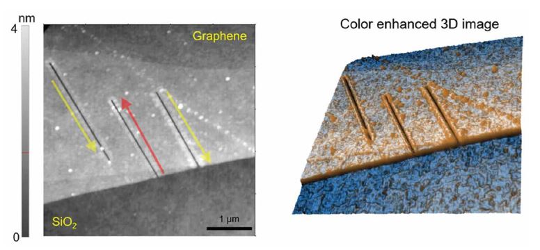
Figure 6. Cutting direction analysis with AFM tip approach speed. When the approach speed is sufficiently slow, the cutting direction does not need to be considered.
In conclusion, our findings show that graphene cutting using the Bias mode of AFM-based nanolithography can be effectively achieved when the AFM tip approaches the sample surface very slowly, allowing adequate time for a water bridge to form between the tip and the surface, with a bias of 3 V or higher, and under a humidity level of 60% or more. This method is effective for both simple line patterns and more complex geometries, as demonstrated in Figure 7.
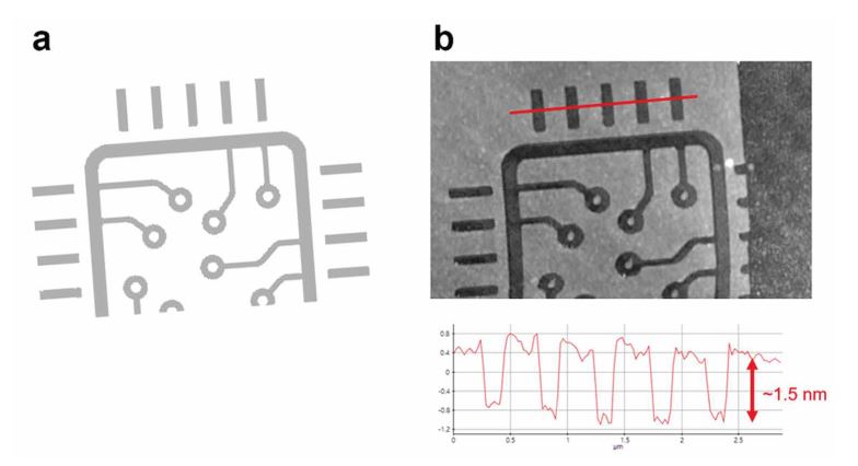
Figure 7. AFM result of graphene patterning from original image by the Bias mode of AFM-based nanolithography.Original image (a) and AFM image (b).
Conclusions
This study demonstrates the effectiveness of AFM-based nanolithography, specifically the Bias mode, for achieving precise nanopatterning on a single layer of graphene. We examined two approaches for AFM-based nanolithography: the mechanical (Set Point/Z scanner mode) and chemical (Bias mode) methods. While mechanical cutting can achieve direct physical etching, it is prone to issues such as unintended damage to the surrounding graphene. The Bias mode, however, proved to be more favorable for graphene nanopatterning due to its ability to induce controlled oxidation using an electric field, thus minimizing physical stress on the AFM tip and allowing for smoother, more precise cuts. Through systematic exploration of key parameters—including applied bias, AFM tip approach speed, and humidity conditions—we identified optimal settings for controlled graphene cutting. These results contribute to a deeper understanding of AFM-based nanolithography on graphene, providing a practical framework for optimizing parameters to achieve high-fidelity patterns. These insights support the development of advanced graphene applications in nanoelectronics, sensors, and other fields requiring high-resolution patterning.
Related Contents

Solving Thin-Film Uniformity Challenges on Curved Surfaces with Imaging Spectroscopic Ellipsometry

Spectroscopic Imaging Ellipsometry at Cryogenic Temperatures Applied to Atomically Thin Crystals