


Moiré imaging with conductive atomic force microscopy
J. Kerfoot1*, V. V. Korolkov1
1Park Systems UK Ltd, MediCity Nottingham, D6 Thane Rd, Nottingham, UK, NG90 6BH
*pse@parksystems.com
Introduction
Conductive AFM (C-AFM) is a technique capable of acquiring current maps with nanometre scale spatial resolution and picoamp scale resolution in current. As the flow of current is fundamental to numerous technologies from computation to energy harvesting, C-AFM has many applications not only for fundamental research but also in the refinement of devices and failure analysis. Here we exemplify the exceptional resolution of C-AFM by studying twist-controlled layered materials heterostructures.
When two rigid layers with a fixed spatial periodicity are overlaid, a moiré pattern may be observed. The symmetry of such features is dependent upon the symmetry of the overlaid layers and the periodicity is dependent upon the mismatch in period Moiré imaging with conductive atomic force microscopy of the two features and the angle between them. Recently moiré patterns have received significant interest for their influence over the functional properties of layered materials heterostructures, namely the field of twistronics [1,2].
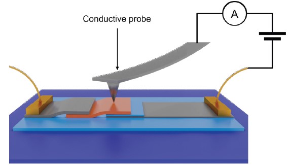
Figure 1. A simplified schematic of C-AFM, in which the interaction between the tip and sample is controlled by either contact mode or PinPointTM AFM. In addition to extracting the topography, a map of the current at the junction between the tip and sample is also extracted.
One prominent example of where moiré patterns have been explored in layered materials heterostructures is the case of single layer graphene (SLG) on hexagonal boron nitride (hBN), where using hBN as a substrate [3] and encapsulant [4] of SLG enables the fabrication of devices in which the effects of contaminant induced doping is suppressed, yielding state-of-the-art performance characteristics such as mobility. For SLG on hBN, a hexagonal moiré pattern is seen owing to the hexagonal symmetry and small spatial mismatch between hBN and SLG (~ 2%), see figure 2 b-d. Samples were fabricated by exfoliating both hBN (HQ graphene) and graphene on thermally grown SiO2 before flakes were sequentially picked up and transferred onto pre-deposited contacts using polymeric stamps. After removing polymer residue through solvent immersion and then mechanically by performing contact mode AFM over the area of interest, samples were measured using C-AFM on the Park FX40 Automatic AFM with Multi75E probes, see fig. 2 e and f.
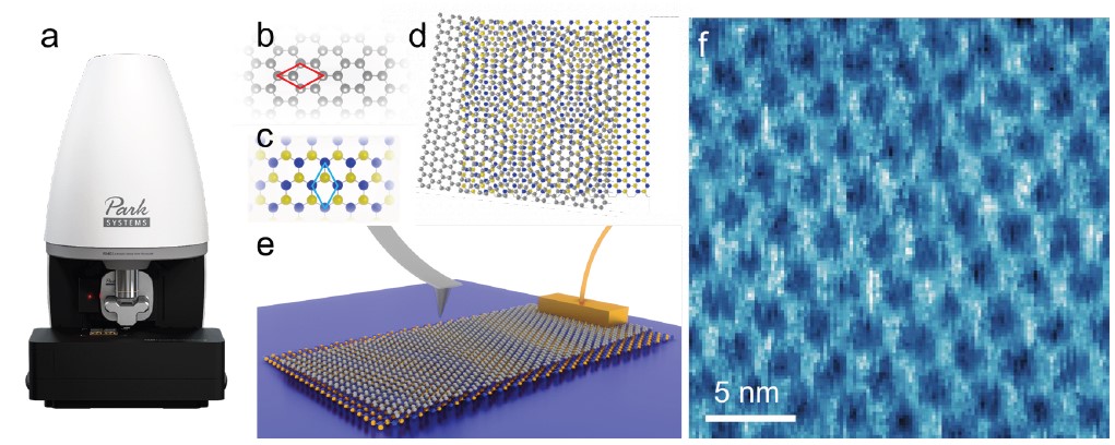
Figure 2. Using the Park Systems FX40 Automatic AFM (a), C-AFM measurements were performed in contact mode to map the morphology of moiré patterns. A heterostructure of SLG (b) on hBN (c) was produced by stacking mechanically exfoliated flakes. The similar lattice constants of hBN and SLG give rise to a moiré pattern, as depicted for a twisted heterostructure (d). With an electrode applied to the substrate and the tip-sample interaction controlled via contact mode (e), current maps acquired under constant voltage may be measured (f) which reveal a hexagonal moiré pattern due to the spatially modulated stacking registry of hBN and SLG.
Experimental and results
C-AFM utilises the same setup as contact mode AFM (with associated mechanical setpoint: SPMech) to maintain the tip in contact with the surface under constant mechanical load via a feedback loop which also allows the topography to be extracted. By applying an electrical contact to the sample and using a conductive probe, the current may be measured at the tip-sample junction and mapped spatially with sub-nanometre resolution. Such current maps of SLG/hBN (see figure 2f and 3a) reveal a hexagonal moiré pattern with areas of higher current observed for the network of walls between domains compared to the central regions where the lattices stack in a more parallel fashion [5,6]. The contrast of such features in AFM images may be optimised by optimising SPMech, the voltage applied between the tip and sample (VTS), increasing the scan rate to suppress thermal drift and changing the state of the tip by applying short and controlled pulses of higher voltage. Upon optimisation of the aforementioned acquisition parameters, current maps showing nanometre scale corrugations (see figure 3a) may be taken, with extracted line profiles (see figure 3b) showing remarkable conformity.
In general, in layered materials heterostructures, the intra-layer forces arising from bonding within layers are stronger than inter-layer forces arising from van der Waals interactions. For this reason, layered materials heterostructures typically exhibit moiré patterns as the stronger intra-layer interactions yield comparatively rigid layers which are not disrupted even when small relaxations may lead to favourable inter-layer adhesion energies [7]. In some special instances, however, layered materials heterostructures may be formed between layers of the same or similar lattice constant and marginal twist angle (typically < 2°) such that inter-layer interactions are sufficient to induce changes in the intra-layer structure, known as atomic reconstruction and demonstrated for the first time in 2L-MoS2 (0°) by Weston et al [8,9].
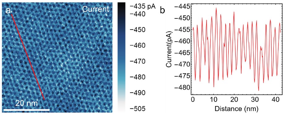
Figure 3. Using C-AFM, a current map (a) of SLG on hBN was measured with VTS = -1 V and SPMech = 2 V (~ 260 nN) with Multi75E cantilevers, showing no contrast in topography but a uniform hexagonal moiré pattern in the current map, as shown in figure 2. To measure the moiré period, a line profile was taken at an angle close to the fast scan direction (b), with an extracted mean spacing of 2.20 nm between local current maxima.
We fabricated such samples using the so-called ‘tear and stack’ method [10], by first exfoliating 1L-MoS2(SPI supplies) on polydimethylsiloxane (PDMS) using scotch tape. The flake was then brought partially into contact with a freshly cleaved highly oriented pyrolytic graphite (HOPG) surface and retracted, such that the flake broke, with part left on the HOPG before the remaining 1L-MoS2 on PDMS was aligned to the first flake and stacked on top. By breaking and restacking the same flake, the twist angle between two layers can be controlled deterministically (0° was used here). Before measuring using C-AFM, samples were annealed to 150 °C for 5 minutes in air before cooling to room temperature and scanned using contact mode AFM to promote the removal of contamination from the top MoS2 surface and buried interfaces.
The cleaned 2L-MoS2 (0°) on HOPG was measured using C-AFM (see figure 4) with VTS = -0.5 V and SPMech = 0.5 V (~ 65 nN), with regular triangular domains observed in both the current and lateral force channels (see figure 4 d and e) but not in topography (see figure 4c). Contrast between current of domains with ‘AB’ and ‘BA’ stacking registries was in good agreement with observations in the literature [8,11]. In addition to the current map, contrast was measured in the lateral force image (the deflection of the cantilever parallel to the scan direction and perpendicular to the cantilever) which implies differences in the mechanical interaction between the tip and 2L-MoS2 across different domains.
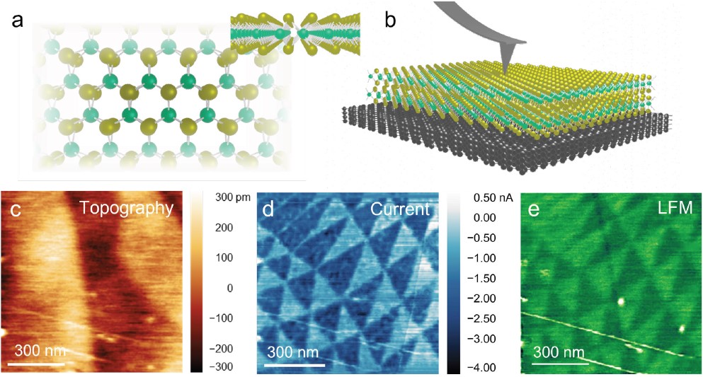
Figure 4. By deterministically breaking and re-stacking a single mechanically exfoliated 1L-MoS2 (a) on HOPG, parallel stacked (0°) registries of 2L-MoS2 can be studied using C-AFM (b). While no contrast is observed in the topography channel (c), regular triangular patterns are observed in both the current map (d) and lateral force map (e) due to differing stacking registries.
Comparing different areas of the same 2L-MoS2 (0°) on HOPG sample, areas of comparatively regular triangular domain morphology (see figure 4d) are observed in addition to more distorted structures (see figure 5a), which we attribute to uneven distributions of strain induced mechanically during sample fabrication. In addition to measuring the morphology of such domains, C-AFM allows the current-voltage characteristics of the junction between the tip and sample to be measured from isolated locations. By performing arrays of point current-voltage measurements across a pre-mapped region, current voltage maps from specific domains may be measured, as shown in figure 5b, to isolate the properties of specific registries and gain insights into how local variations affect the performance of completed devices.
Conclusion
In conclusion, we have demonstrated that C-AFM enables spatially modulated functional properties in electrically conductive samples to be measured with nanometre scale resolution and highly relevant functional properties to be measured via mapping and spectroscopy. The advantage of C-AFM is that it provides information on the electrical properties of materials at nanometre length scales which are complementary to both optical spectroscopy and device characterisation techniques, which is valuable both in exploring the fundamental properties of twisted layered materials heterostructures and in the optimisation of devices such as transistors, memristors, photodetectors and light emitting diodes.
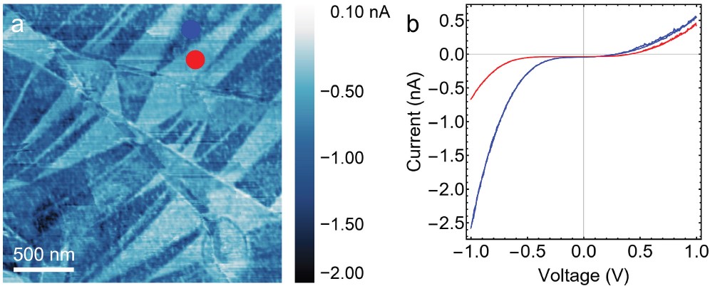
Figure 5. For the same parallel stacked 2L-MoS2/HOPG sample shown in figure 4, a larger area current map was measured, revealing less regular distorted domains (a). By positioning the probe over specific domains, current-voltage curves may be measured (b), revealing differing characteristics over regions of high and low current contrast
References
[1] R. Ribeiro-Palau et al. Science 361, 6403, 690 (2018).
[2] Y. Cao et al. Nature 556, 80 (2018).
[3] C. Dean et al. Nat. Nanotechnol. 5, 722 (2010).
[4] D. G. Purdie et al. Nat. Commun. 9, 5387 (2018).
[5] C. Woods et al. Nature Phys. 10, 451 (2014).
[6] A. Davies et al. Nano Lett. 18, 1, 498 (2018).
[7] V. V. Enaldiev et al. PRL 124, 206101 (2020).
[8] A. Weston et al. Nat. Nanotechnol. 15, 592 (2020).
[9] A. Weston et al. Nat. Nanotechnol. 17, 390 (2022).
[10] K. Kim et al. Nano Lett. 16, 3, 1989 (2016).
[11] M. R. Rosenberger et al. ACS Nano 14, 4, 4550 (2020).