


Jay Son,1 Edward Park,1 Luna Kim,1 John Park1 and Charles Kim1
James Kerfoot,2 Andrea Cerreta2
1Park Systems, HQ, Suwon, Republic of Korea
2Park Systems GmbH, Europe, Mannheim, Germany
Introduction
As research on next-generation semiconductor devices and 2D material–based electronics continues to advance, there is a growing demand for integrated platforms capable of simultaneously probing electrical properties and surface/interface characteristics with nanoscale precision1,2. In particular, performing advanced AFM modes under applied source–drain and back-gate bias requires reliable multi-electrode probing that can be combined with AFM scanning without mechanical or electrical interference3,4.
However, conventional AFM systems often rely on external probe stages or manual probing setups, which complicates the experimental configuration, reduces reproducibility, and increases the likelihood of mechanical interference during high-resolution scans. Additionally, the use of heavier mechanical manipulators can impose added weight on the scanner, introduce uncontrolled mechanical load on the sample, and limit placement accuracy in XYZ, all of which can further compromise stable, high-resolution AFM measurements.
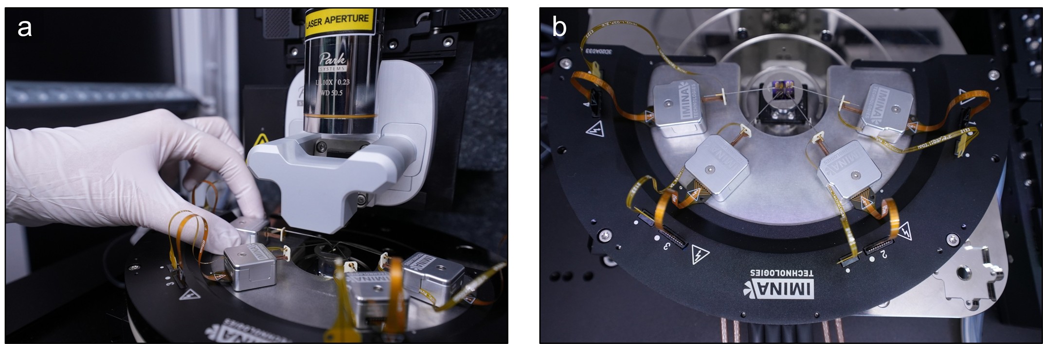
Figure 1. l Integrated configuration of the Park Systems FX200 AFM and the Imina Technologies Microprobing Platform (4-Bot).
(a) Photograph of the Imina Technologies Microprobing Platform (4-Bot) installed inside the Park Systems FX200 AFM, and (b) top view of the integrated setup. Up to four miBot units can be placed on the sample stage without mechanical interference with the AFM head or the cantilever.
To address these challenges, Park Systems and Imina Technologies present a solution that fully integrates the Imina Technologies Microprobing Platform (4-Bot) into Park Systems AFM instruments. As illustrated in Figure 1-a, the probe station can be mounted directly on the FX200 sample chuck, allowing electrode probes to be positioned precisely near the region of interest without interfering with the
AFM cantilever, while each miBot is magnetically anchored to the stage for easy manual attachment and removal. Furthermore, up to four miBot units (Figure 1-b) can be used simultaneously and controlled independently with micrometer-scale precision. By combining this configuration with the auxiliary in/out channels of the Park Systems AFM controller, the integrated platform enables multi-electrode
contact, real-time biasing, and high-resolution AFM-based nano-imaging within a single unified system.
Hardware Setup
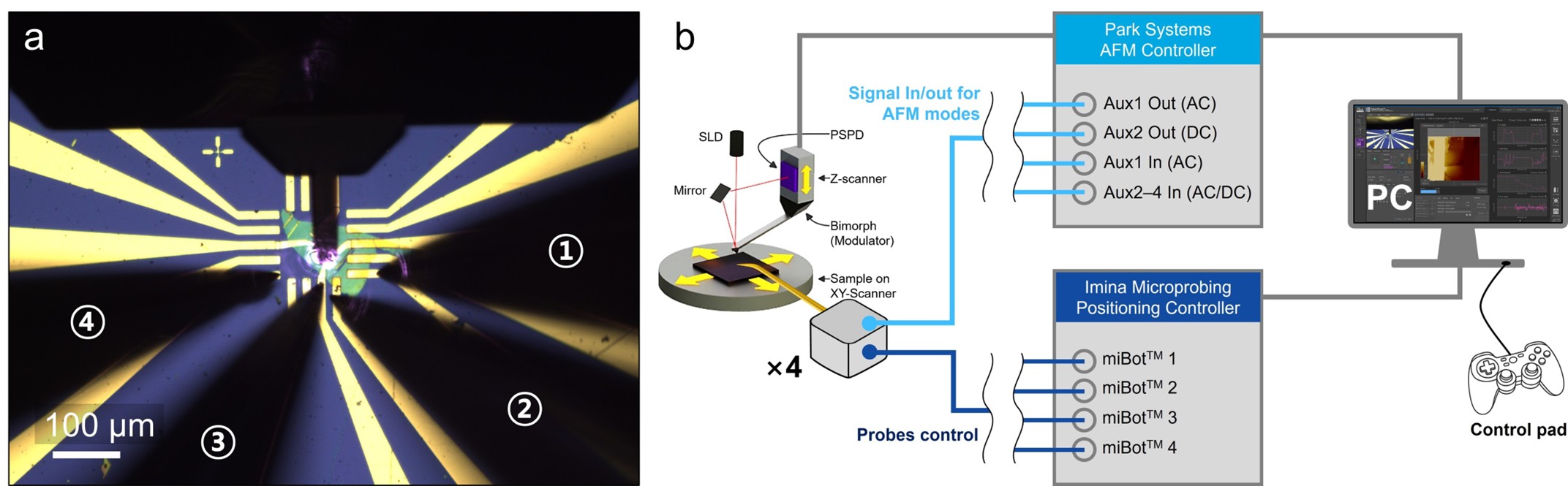
Figure 2. l Multi-probe arrangement inside the Park Systems FX200 AFM, and signal & control configuration.
(a) Optical image of a device with patterned gold electrodes loaded into the Park Systems FX200 AFM, acquired using the built-in vision system. Four tungsten probes mounted on miBot units are positioned on the targeted electrode pads in the vicinity of the AFM cantilever, enabling AFM measurements without mechanical interference with the individual probes. (b) Schematic diagram of the operating configuration in which the probe station is integrated with the AFM system. Each miBot is connected via two separate communication lines to the AFM controller and the positioning controller, respectively. The tungsten probes mounted on the miBot units are interfaced with the Aux1 and Aux2 Out channels of the AFM controller to apply AC/DC drive signals to the device, and with the Aux1 In and Aux2–4 In channels to acquire AC or AC/DC measurement signals. Up to four miBot units can be used simultaneously and are finely positioned by the positioning controller, while a PC-connected control pad provides an intuitive interface for independent probe manipulation.
In this work, applications where advanced AFM modes on sample of different nature are made possible via the use of a variable number of contacts will be discussed. The hardware setup was configured by integrating a Park Systems FX200 AFM with the Imina Technologies Microprobing Platform (4-Bot) kit.
As an example, in Figure 2 it is shown a device with patterned gold electrodes which was loaded onto the FX200 sample stage. At first, the AFM cantilever was positioned in close proximity to the region of interest. After that, the tungsten probes were carefully positioned onto the source, drain, and auxiliary contact pads of the device to ensure that their placement did not obstruct or perturb the AFM cantilever during subsequent scanning. The alignment procedure was conducted effortlessly due to the high-resolution optical capabilities of the AFM system and the intuitive operation of the Precisio™ software.
As schematically summarized in Figure 2-b, the electrical configuration was arranged such that the Aux1 and Aux2 Out channels of the AFM controller supplied AC/DC drive signals to the device, while the Aux1 In and Aux2–4 In channels were used to collect the AC and AC/DC electrical responses generated by the device. The positions of the miBot units were controlled via a dedicated positioning controller and a PC-connected control pad, allowing independent adjustment of the speed and direction of each probe and thereby enabling stable electrical contact and four-probe configurations synchronized with AFM measurements.
Figure 2 gives an overview of the possible use of the integrated system to probe the sample response to simultaneous AC and DC biasing. In the following sections, the actual number of tungsten probes used for the experiments and the signals carried through them will be explained.
Performing Electrical AFM on electrically floating LMs and LMHs
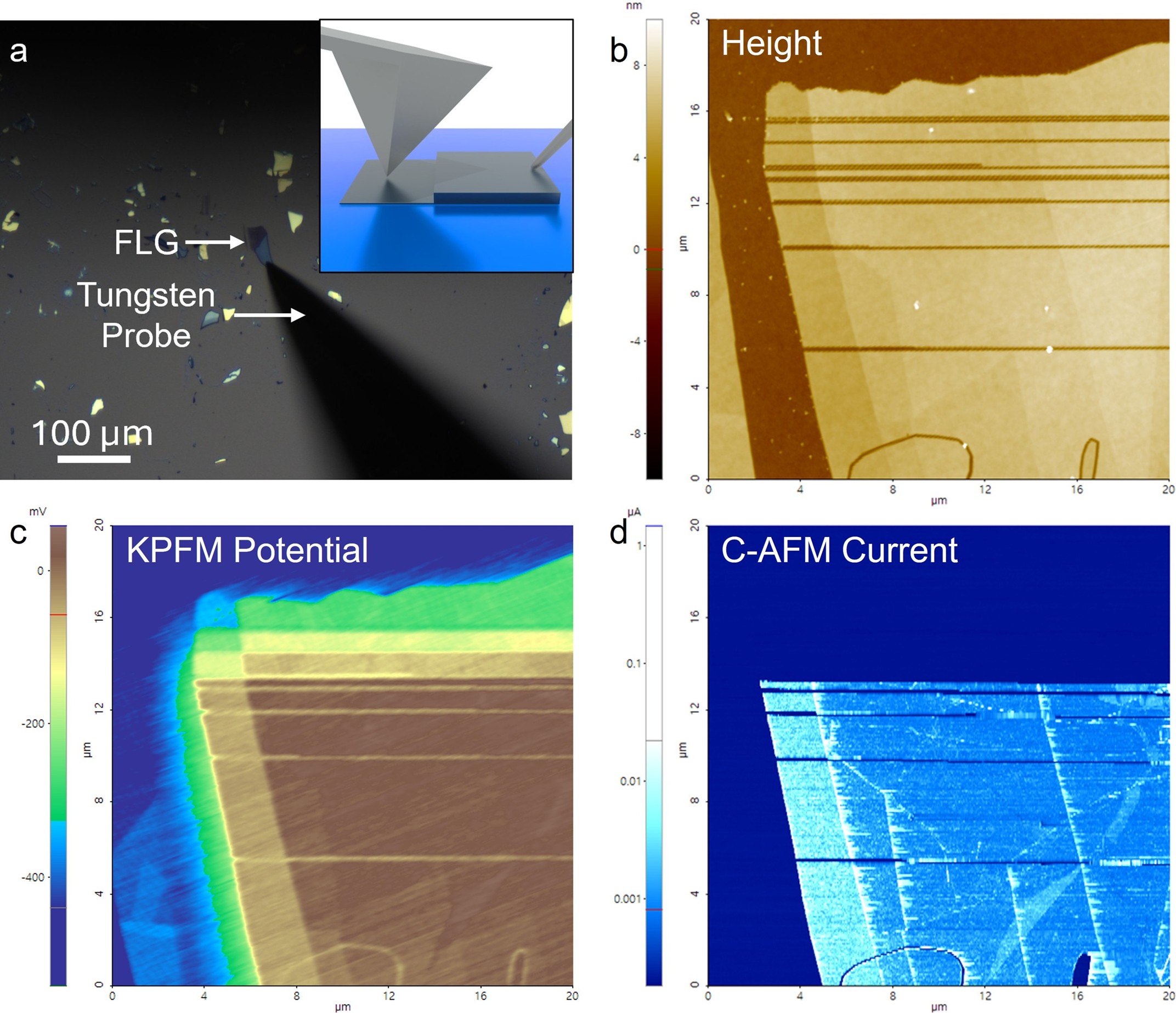
Figure 3. l Contact-enabled HD-KPFM imaging and current mapping of FLG.
(a) An optical view from the FX200 camera showing a tungsten probe touching a graphite flake connected to FLG, with a schematic inset. (b) Non-contact mode height images of the FLG flake showing the height in addition to patterning achieved by anodic oxidation. (c, d) The electrical contact to the FLG enabled the acquisition of both stable single-pass HD-KPFM imaging over the contacted FLG in addition to maps of the current flow over different regions of the FLG.
Electrical AFM modes offer the possibility to characterize layered materials (LMs) and layered material heterostructures (LMHs) with excellent spatial resolution, with examples being the observation of moiré patterns in conductive AFM and moiré superlattices in marginally twisted heterostructures of MoS2 and hBN with Kelvin probe force microscopy (KPFM)5. One drawback of these techniques however, is
that they require electrical contacts, which typically necessitates lithography and deposition of metal contacts, and cannot be used to monitor LMHs during their fabrication6. Here we show that the miBot units enable individual flakes of LMs on insulators to be electrically contacted and studied using electrical AFM.
Figure 3-a shows the camera view of the FX200 with the probe withdrawn and a miBot used to electrically contact an area of graphite attached to a few layered graphene (FLG) flake. The miBot contact was used as act as a ground to prevent the accumulation of charge that would inhibit single-pass KPFM measurements as well as acting as a drain in C-AFM. To elucidate the grounding effect, channels
were patterned into the FLG flake by local anodic oxidation. The top three cuts bisected the flake completely, rendering them electrically floating versus the remaining region of FLG contacted to the miBot. As can be seen in figure 3 panels c and d, the isolated regions of FLG possessed a differing potential which is indicative of charging while showing no current in C-AFM.
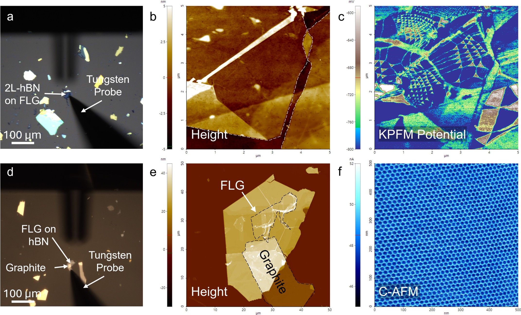
Figure 4. l Contact-enabled HD-KPFM imaging and C-AFM moiré mapping of hBN/FLG heterostructures.
(a, b, c) A parallel stacked hBN homostructure on an underlying FLG on 90 nm SiO2 exhibiting a ferroelectric superlattice was contacted by a miBot before being measured by non-contact mode height and HD-KPFM potential, again revealing the absence of charging. (d, e, f) The utility of the technique was further exemplified by contacting an FLG flake on hBN on a mica/PDMS stamp prior to non-contact mode and C-AFM imaging revealing a moiré pattern between the FLG and hBN.
Having established the ability of the nanobot to contact individual LM flakes, we demonstrate its ability to enable more sophisticated electrical characterization without the need for special substrate configurations or patterning of contacts. In the tip row of figure 4, we demonstrate heterodyne (HD-) KPFM measurements of a ferroelectric superlattice formed between two parallel stacked hBN flakes on FLG
on 90 nm SiO2. These high-resolution single-pass measurements are facilitated by the grounding contact made by the miBot, as the bias applied to the tip in KPFM would be sufficient to charge the flake and give rise to a drift in the KPFM potential. In a second example, we apply an electrical contact to FLG aligned to a ~25 nm thick hBN flake on a mica membrane on PDMS to measure a moiré pattern in
C-AFM, as shown in the bottom row of figure 4. The mica membrane on PDMS was used to pick up the hBN and FLG flakes and acted as the stamp in the LMH fabrication, hence demonstrating that the miBot enables the electrical characterization of LMHs on stamps during fabrication. This innovation enables both the characterization of interfaces that may become buried during later fabrication steps and the ability to verify the registry of layers in heterostructures – reducing instances of expending valuable nanofabrication time on misaligned
heterostructures.
In-operando KPFM on UV-ozone treated MoS2 device
Samples used for these tests were kindly provided by Prof. Young-Jun Yu, Chungnam National University, Republic of Korea, and was prepared by selectively oxidizing a portion of the MoS2 surface, to form UV-ozone-treated two-dimensional semiconductor MoS2 similar to the ones described in reference 9.
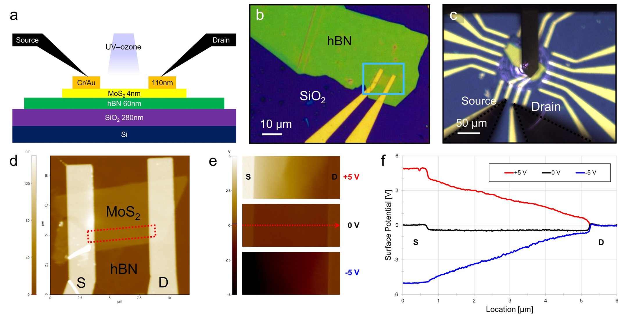
Figure 5. / KPFM measurements of a UV-ozone-treated MoS2 thin-film device under source–drain bias.
(a) Cross-sectional schematic of the MoS2 thin-film device fabricated for KPFM measurements. (b) Optical microscope image of the fabricated MoS2 thin-film device, where the blue box indicates the MoS2 channel region used for the KPFM measurements. (c) Image acquired via the FX200 camera after loading the sample and approaching the dedicated KPFM cantilever to the device for surface potential measurements. (d) AFM height image of the MoS2 device transferred onto the hBN layer. Gold electrodes acting as the source (S) and drain (D) are located on the left and right, respectively, and KPFM measurements were performed in the central region indicated by the red dashed box. (e) KPFM surface potential images of the MoS2 channel acquired with a source bias equal to +5, 0 and -5 V DC
(from top to bottom) and with the drain electrode held at ground (0 V). (f) Line profiles of the KPFM surface potential.
KPFM measurements on UV-ozone-treated MoS2 thin-film devices were performed under the structural and biasing conditions summarized in Figures 53,4. A ~60 nm-thick hBN flake was first dry-transferred onto a Si substrate with a 280 nm thermal SiO2 layer, and an ~4 nm-thick exfoliated MoS2 flake was subsequently transferred in an island-like geometry on top of the hBN. Cr/Au (10 nm/100 nm) electrodes were then patterned by electron-beam lithography and metal deposition to define the source and drain contacts (Figures 5-a and 5-b)1,2. UV-ozone treatment was applied locally on the completed device in order to induce partial oxidation within selected regions of the MoS2 channel5–7.
The sample was then loaded the AFM microscope, where two tungsten probes mounted on miBot units were brought into contact with the source and drain pads, and the AFM cantilever (NSC36/Cr-Au-B) was approached above the MoS2 channel to perform KPFM surface potential imaging (Figures 5-c and 5-d). During the measurements, the drain electrode was kept at ground (0 V), while a DC bias −5 V, 0V, +5 V was sequentially applied to the source electrode. For each bias condition, KPFM surface potential maps were acquired over the boxed region indicated by the red dashed outline in Figure 5-d. Figure 5-e shows KPFM surface potential images of the MoS2 channel acquired at each source voltage. The slope and overall shape of the potential profile depend on both the magnitude and polarity of the applied bias. This behavior is quantified in Figure 5-f, which overlays the surface potential line profiles extracted along the source–channel–drain direction indicated by the red dashed arrow in Figure 5-e: at the source electrode the applied bias is faithfully reproduced in the measured potential, an almost linear potential drop is observed across the channel.
This miBot-integrated in-operando KPFM approach offers the advantage of quantitatively extracting the contact resistance (and its asymmetry) and mapping the voltage-drop distribution along the channel by comparing measurements acquired under varied source–drain bias configurations (polarity and magnitude), while directly localizing edge-related effects and other spatially confined changes in resistance. Furthermore, combining KPFM mapping with electrical sweeps (I–V and gate-voltage-dependent measurements) helps establish correlations between spatially resolved surface-potential landscapes and the device transport characteristics.
SThM on nano-structured devices
Samples used for these tests were kindly provided by Dr. Akash Kumar, University of Gothenburg, Sweden, and consist of geometrical structures connected by nano-constrictions, to form spin Hall Nano-oscillator chains similar to the ones described in reference 12. Single or multiple repetitions of such structures are electrically connected to large top and bottom electrodes. Via contacting each of these
electrodes with a tungsten probe, it is possible to allow the passage of current through the device (Figure 6-a).
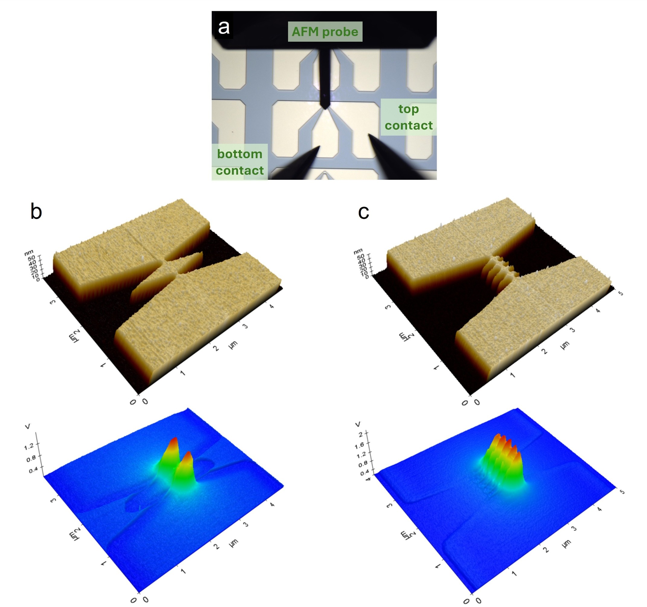
Figure 6. / Thermal mapping of nano devices.
(a) Structures consist of a chain of nano-constrictions which are in electrical contact with a top and bottom pad, each one contacted via a needle probe. (b) Topographical map of a device with two nano-constrictions (top) and relative SThM map (bottom), where higher SThM voltage indicates a higher temperature. The same applies to (c) where a structure with five nano-constrictions was probed. For both (b) and (c), topography was mapped by means of a PPP-MFMR probe (Nanosensors) in non-contact mode, while SThM maps were obtained using a VTP-200 probe and the VertiSense™ setup from AppNano, with a constant current of 2 mA applied through the needles interfaced with a Keithley 2636B source meter.
Scanning Thermal Microscopy (SThM) experiments were performed using the AppNano VertiSense™ module, with proprietary thermocouple-based AFM probes. The voltage measured by the thermocouple can be converted to temperature after a calibration procedure. AppNano probes can be provided on carrier plates compatible with the Park Systems probe mounting.
Experiments were carried out on a Park Systems FX200 AFM tool. A Keithley 2636B source meter was used in its current generator configuration to provide constant DC current to the devices via the Imina probes during the experiments. The SThM maps recorded while a constant 2 mA DC current circulates through the devices show peaks of intensity in correspondence of the nano-constrictions, where
higher current density is expected.
This miBot-enabled SThM approach offers the advantage of directly localizing Joule-heating hotspots and quantifying their relative intensity by comparing thermal maps acquired under controlled DC current injection, thereby highlighting nano-constrictions where current crowding is most pronounced. In particular, systematic variation of the drive current can be used to track how the thermal response evolves with electrical loading and to reveal constriction-to-constriction non-uniformities, which may indicate locally increased resistance or imperfect electrical connectivity.
Conclusions
This application note demonstrates that integrating a Park Systems FX200 AFM with the Imina Technologies Microprobes (4-Bot) offers a single platform for the performance of advanced electrical AFM modes in-operando and in concert with global device behavior and conventional high-resolution AFM imaging. By precisely aligning miBot-mounted tungsten probes and the AFM cantilever inside the
FX200, stable source–drain biasing can be applied without mechanical interference during KPFM and SThM measurements. Firstly, the ability of the miBot to apply an electrical contact at specific locations enables individual LM flakes and LMHs to be addressed with electrical AFM with greatly improved experimental flexibility. For UV-ozone-treated MoS2 devices, bias-dependent KPFM measurements reveal changes in the potential landscape across the interface to electrodes and within the channel. For nano-structured devices, SThM mapping of constant DC current-dependent Joule heating visualizes the spatial distribution of heat generation and enables thermal analysis of the channel properties. These results demonstrate that the combination of Park Systems AFM and the Imina Technologies platform provides a powerful and flexible solution for nanoscale electrical and thermal characterization of 2D materials and thin-film electronic devices.
1. Wang, Qing Hua, et al. "Electronics and optoelectronics of two-dimensional transition metal dichalcogenides." Nature nanotechnology 7.11 (2012): 699-712.
2. Schwierz, Frank, Jörg Pezoldt, and Ralf Granzner. "Two-dimensional materials and their prospects in transistor electronics." Nanoscale 7.18 (2015): 8261-8283.
3. Melitz, Wilhelm, et al. "Kelvin probe force microscopy and its application." Surface science reports 66.1 (2011): 1-27.
4. Wagner, Tino, et al. "Kelvin probe force microscopy for local characterisation of active nanoelectronic devices." Beilstein journal of nanotechnology 6.1 (2015): 2193-2206.
5. Sequeira, Ian, et al. "Manipulating moires by controlling heterostrain in van der Waals devices." Nano Letters 24.49 (2024): 15662-15667.
6. Vizner Stern, Maayan, et al. "Interfacial ferroelectricity by van der Waals sliding." Science 372.6549 (2021): 1462-1466.
7. Ma, Xiaolei, et al. "Defects induced charge trapping/detrapping and hysteresis phenomenon in MoS2 field-effect transistors: mechanism revealed by anharmonic Marcus charge transfer theory." ACS Applied Materials & Interfaces 14.1 (2021): 2185-2193.
8. Park, Youngseo, et al. "Thermally activated trap charges responsible for hysteresis in multilayer MoS2 field-effect transistors." Applied Physics Letters 108.8 (2016).
9. Shin, Beomkyu, et al. "Half-Oxidized MoS2-Based Memristor by UV-Ozone Treatment." ACS Applied Electronic Materials 7.9 (2025): 3737-3743.
10. Bodzenta, Jerzy, and Anna Kazmierczak-Bałata. "Scanning thermal microscopy and its applications for quantitative thermal measurements." Journal of Applied Physics 132.14 (2022).
11. Tovee, Peter D., et al. "Nanoscale resolution scanning thermal microscopy using carbon nanotube tipped thermal probes." Physical Chemistry Chemical Physics 16.3 (2014): 1174-1181.
12. Kumar, Akash, et al. "Robust mutual synchronization in long spin Hall nano-oscillator chains." Nano Letters 23.14 (2023): 6720-6726.
Application
Related Products
Related Modes
Related Contents

Solving Thin-Film Uniformity Challenges on Curved Surfaces with Imaging Spectroscopic Ellipsometry
Spectroscopic Imaging Ellipsometry at Cryogenic Temperatures Applied to Atomically Thin Crystals