Layer-controlled epitaxy of 2D semiconductors: bridging nanoscale phenomena to wafer-scale uniformity


- Journal: Nanotechnology
- Published Year: 2018
- Authors: Daniele Chiappe, Jonathan Ludwig, Alessandra Leonhardt, Salim El Kazzi, Ankit Nalin Mehta, Thomas Nuytten, Umberto Celano, Surajit Sutar, Geoffrey Pourtois, Matty Caymax
- Application: nanoelectronics, optoelectronics, TMDs
Summary
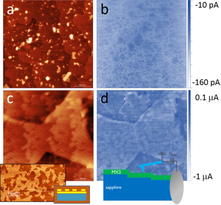
Researchers from imec and Uni Leouven report a method for layer-controlled epitaxy of MoS₂ using MOCVD, enabling uniform, wafer-scale growth without alkali metal promoters. By tuning temperature and H₂ flow, they control lateral growth and activate selective thermal etching to remove excess layers. Conductive AFM (C-AFM on NX-Hivac Vacuum AFM) was used to analyze morphology and local conductivity. C-AFM confirmed enhanced electronic properties in films grown with the etching-based method. The work advances scalable synthesis of 2D TMDs with improved structural and electrical performance for future nanoelectronic applications.