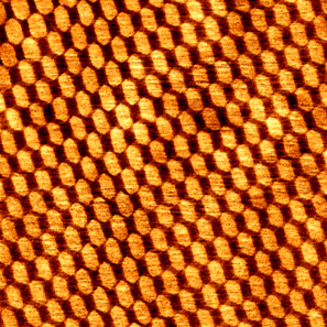
e-Beam Damage on ArF Photo Resist
This slide shows e-beam damage on ArF photoresist.
The AFM topography image reveals surface modifications caused by e-beam exposure.
The PiFM image highlights compositional changes in the exposed regions, clearly distinguishing them from the unaffected areas.
Scanning Conditions
- System: Nano-IR
- Sample: Sample: PR pattern sample
- Scan Mode: PiFM (Channel: Z Height, PiFM Amplitude)
- Scan Rate: 1 Hz
- Scan Size: 1 µm × 1 µm
- Pixel Size: 512 × 256 pixels
Related Contents
Publications
Three-Dimensional Nanoscale Control of Magnetism in Crystalline Yttrium Iron Garnet
Publications
Probing the DOS Band Tail in Amorphous Thin-Film Transistors via Capacitance–Voltage Analysis
Publications
Desired Location Doping in 2D Semiconductors via Bottom- Patterned Ultrathin Nafion for Stable and Excessive Hole-Carrier Supply
×