


Nano Materials
Patterned Arrays of Magnetic Nanostructure
Patterned arrays of magnetic nanostructures have become one of the key issues in recent years because of its potential application to information technology with respect to magnetic storage devices. Particular attention has been given to the magnetic properties of periodic arrays of micron and submicron elements of very different shapes, especially dots and stripes. The study of these arrays of submicron elements is the basis for the development of magnetic memories and nanopatterned recording media, since the inter-element interaction determines the integration limits of magnetic memories and nanopatterned recording media.
The periodic magnetic domain structure was observed by using a magnetic force microscopy (MFM). The method was the first scanning probe technique and turned out to be a powerful tool for submicron-scale magnetic image mapping. In order to measure the magnetic properties of periodic structures based on magnetic/nonmagnetic films, the MFM technique is better suited that possess the high sensitivity required to monitor magnetic domain structure in thin films and very small elements of different shapes.
We fabricated two-dimensional (2D) Co magnetic arrays by the photolithography with KrF laser source and the wet etching (Transene Inc., TFB) process. A Co film, 40 nm thick, was deposited on a 6-inch Si(100) wafer by using a sputtering system.
The magnetic domain structure has been investigated using a MFM system, which is basically a scanning probe microscopy (Park SYSTEMS, XE-100) equipped with a magnetic tip (Nanosensors, PPP-MFMR). Also, the MFM system was equipped with an electromagnet, which allows us to investigate the evolution of the magnetic domains in an in-plane applied magnetic field.
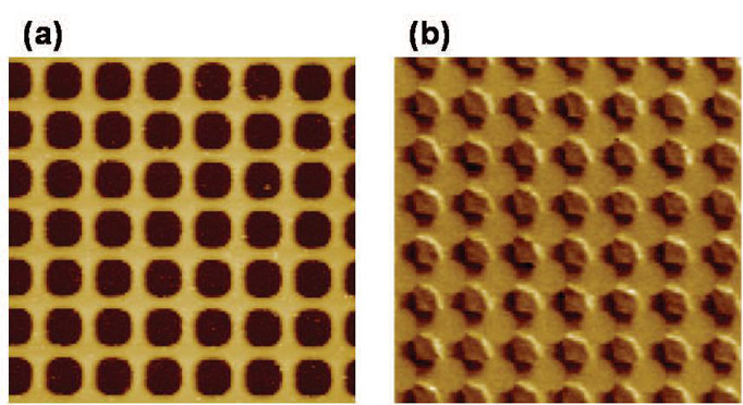
FIG. 1: (a) AFM and (b) MFM images of 2D patterned arrays of Co antidot structures. The scan area is 10 μm x 10 μm.
Figure 1 shows the atomic force microscopy (AFM) and the MFM images obtained from 2D patterned arrays of Co antidote structures. The MFM image in Fig. 1(b) has three different domains. Two are wedge-shaped domains connecting the holes and the other is a diamond-shaped domain. For the wedge-shaped domains, the magnetization vector is parallel to the connecting boundaries at the holes and points from dark to bright inside the domain. The magnetization vector in the diamond-shaped domain is oriented along the diagonal. This configuration minimizes the magnetostatic energy.
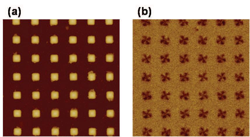
FIG. 2: (a) AFM and (b) MFM images of 2D patterned arrays of Co dot structure. The scan area is 10 μm x 10 μm.
As shown in Fig. 2(a), the AFM image study reveal that a 2D patterned arrays of submicron square dot structures was fabricated. The AFM image clearly shows a square-lattice pattern with a periodicity of about 1.6 μm. By comparing the AFM and the MFM images [see Fig.2(a) and Fig. 2(b), respectively], it is clear that the topography and the magnetic contrast are well separated. The MFM image of the square pattern shown in Fig. 2(a) demonstrates a Landau-Lifshitz-type flux closure domain structure with 90° domain walls and a central vortex. The magnetic charges are mainly concentrated along the domain walls. In systems with a negligible magnetocrystalline anisotropy, the balance of demagnetization and exchange energies results in flux-closure structures such as four fold-closure-domain pattern in thin squares. It can be seen that, apart from the contrast associated with domain walls, the one related to the vortex core is also clearly detected.
As seen in Fig. 3, two kinds of vortex chirality appear in all the patterned arrays, namely clockwise and counter-clockwise, with an approximately equal probability due to the two fold energy degeneracy. This finding reveals the bistability of magnetic vortices and the statistically random distribution of vortex chirality. Additionally, the vortices of different chiralities present clearly the corresponding MFM images under an applied field.
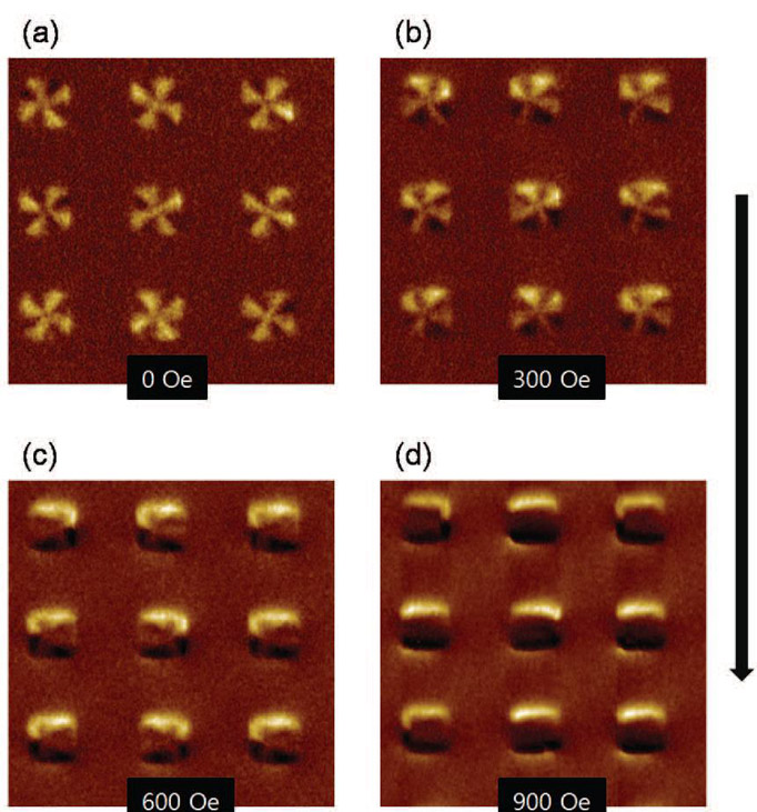
FIG. 3: Field-dependent MFM images of square Co dots. The scan area is 5 μm x 5 μm .
The field-dependent MFM images show that the application of the field (indicated by a black arrow) induces the domain-wall motions (see Fig. 3). The intersection moves, first, perpendicular to the applied field direction and gradually approaches the corner. At H = 300 Oe, the field increases the size at the expense of the right (or left) domain. As the strength of applied field keeps increasing, the magnetization vectors are antiparallel to the external field, and eventually all the magnetic moments are reversed and become parallel to the field. As seen in Fig. 3(d), the magnetic domains gradually collapse with each other. These characteristics are closely related to the distribution of vortex annihilation (nucleation) fields.
Nanoparticles/Nanotubes
Mechanical Properties (F-D Spectroscopy)
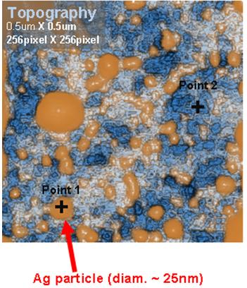
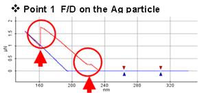
FD spectroscopy on the Ag particle show aberrations associated with the indentation of the nanoparticle.
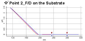 FD spectroscopy on the substrate show no effects of indentation.
Relevant Publications using Park AFM and F-D Spectroscopy
Qihua Xiong, N. Duarte, S. Tadigadapa, and P. C. Eklund; Force-Deflection Spectroscopy: A New Method to Determine the Young’s Modulus of Nanofilaments; Nano Lett., 2006, 6 (9), 1904-1909
Equipment: Park Systems XE-100
Abstract: We demonstrate the determination of Young's modulus of nanowires or nanotubes via a new approach, that is, force-deflection spectroscopy (FDS). An atomic force microscope is used to measure force versus deflection (F−D) curves of nanofilaments that bridge a trench patterned in a Si substrate. The FD data are then fit to the Euler−Bernoulli equation to determine Young's modulus. Our approach provides a generic platform from which to study the mechanical and piezoelectric properties of a variety of materials at the nanoscale level. Young's modulus measurements on ZnS (wurtzite) nanowires are presented to demonstrate this technique. We find that the Young's modulus for rectangular cross section ZnS nanobelts is 52 ± 7.0 GPa, about 30% smaller than that reported for the bulk.
Graphene Membrane/Graphite
Mechanical Properties - Nanoindentation
Graphite is a layered compound composed of carbon atoms. It is important industrially for its electrical and lubricating properties. Graphite is made up of layers of graphene, which is thought to be on of the strongest materials to be tested with a breaking strength 200 times that of steel.
Relevant Publication using the Park AFM and Nanoindentation
Title: Measurement of the Elastic Properties and Intrinsic Strength of Monolayer Graphene
Authors: C. Lee, X.Wei, J.W. Kysar, J. Hone
Journal: SCIENCE 321(18) JULY 2008 p. 385
System: Park Systems XE-100
We measured the elastic properties and intrinsic breaking strength of free-standing monolayer graphene membranes by nanoindentation in an atomic force microscope. The force-displacement behavior is interpreted within a framework of nonlinear elastic stress-strain response, and yields second- and third-order elastic stiffnesses of 340 newtons per meter (N m-1) and -690 N m-1, respectively. The breaking strength is 42 N m-1 and represents the intrinsic strength of a defect-free sheet. These quantities correspond to a Young’s modulus of E = 1.0 terapascals, third-order elastic stiffness of D = –2.0 terapascals, and intrinsic strength of sint = 130 gigapascals for bulk graphite. These experiments establish graphene as the strongest material ever measured, and show that atomically perfect nanoscale materials can be mechanically tested to deformations well beyond the linear regime.
Graphene (Step Height)
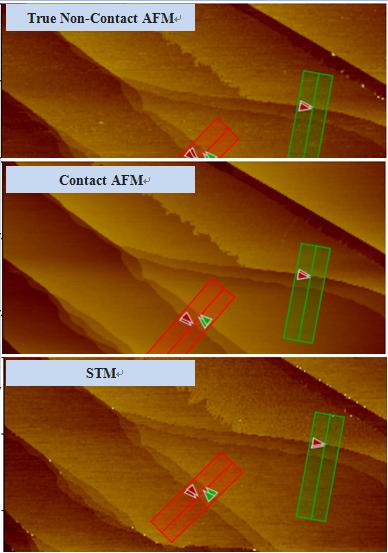
Metrology - (True-NC-AFM, Contact AFM and STM)
 Graphene is a sheet of carbon atoms bound together with double electron bonds (called a sp2 bond) only one-atom-thick. The atoms in graphene are densely packed in a honeycomb style crystal lattice. Graphene is extracted from graphite. Graphite itself consists of many graphene sheets stacked together.
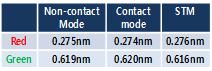
It has been shown that step height measurements taken on graphene sheets show an inconsistency in the reported value. This inconsistency is seen both among different AFMs, as well as, when using different modes on the same AFM. With the Park AFM, inconsistency is removed. The images on the left are of Graphene on SiC imaged by True-Non Contact AFM, Contact AFM, and STM using the Park Systems AFM. The graphene step height measurements show consistent results among the three modes.
Sample: Graphene on SiC
Courtesy of : Georgia Institute ofTechnology.
Image Conditions:
- True Non-Contact
- Contact AFM
- STM
- Scan size (5x2.5 um)
- Scan rate (1Hz)
- Z servo gain (1)
- Pixel (512 x 512)
System Requirement:
- True Non-Contact
- Contact Mode
- STM
- Decoupled XY closed-loop scanner
- Flexure guided Z-scanner with fast response(10kHz)
Thin Film - ZnO
Electrical Property (EFM/KPFM)
The material and electrical properties of Zinc Oxide (ZnO) have made the compound attractive in the area of thin film transistors and light emitting diodes. Due to it non-toxic, wide bandgap and electrical conductivity, it is thought to be ideal for use in solar cell devices.
Publication on ZnO Using KPFM and the Park AFM
DR Doutt C Zgrabik, HL Mosbacker, LJ Brillson; Impact of near-surface native point defects, chemical reactions, and surface morphology on ZnO interfaces; J. Vac. Sci. Technol. B 26,4, Jul/Aug 2008 1477
Equipment: Park Systems XE-70
Abstract: The authors used a complement of depth-resolved cathodoluminescence spectroscopy _DRCLS_, atomic force microscopy _AFM_, and Kelvin probe force microscopy _KPFM_ to correlate the formation of native point defects with interface chemical reactions as well as surface morphology. A wide array of ZnO crystals grown by both melt and hydrothermal growth methods display orders-of-magnitude variation in 2.1, 2.5, and 3.0 eV native point defect optical transitions at their free surface and as a function of depth on a nanometer scale. AFM surface morphology scans taken simultaneously with KPFM potential maps reveal large variations in surface morphology related to the growth method and subsequent processing. Notably, when DRCLS defect emissions are low, the surface roughness is low and the morphology matches its respective KPFM potential map. When DRCLS emissions vary with depth, the morphology and potential maps do not correlate. Indeed, the latter can vary by hundreds of meV across micron square areas. These subsurface electrical changes are consistent with DRCLS features and emphasize the contribution of surface morphology to electrically active interface defects. The relative strength of near band edge to deep level defect emissions exhibit a threshold dependence on surface roughness.
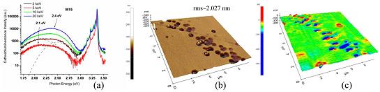
FIG. 3. _a_ DRCLS spectra for hydrothermally grown single crystal ZnO substrate MTI 15 alongside its respective _b_ AFM topography and _c_ KPFM potential map. DRCLS spectra show some of the highest bulk and surface NBE intensities and deep levels at 2.1 and 2.4 eV. The dashed curves represent the Gaussian deconvolution. Its KPFM potential map shows large _hundreds of mV_ potential changes across its surface.