


Semiconductor
How to obtain sample potential data for KPFM measurement
Kelvin Probe Force Microscopy, or KPFM, was introduced as a tool to measure the local contact potential difference between a conducting atomic force microscopy (AFM) tip and the sample, thereby mapping the work function or surface potential of the sample with high spatial resolution. Since its first introduction by Nonnenmacher [1], KPFM has been used extensively as a unique method to characterize the nano-scale electrical properties of metal or semiconductor surfaces and semiconductor devices. Recently, KPFM has also been used to study the electrical properties of organic materials, devices [2–4] and biological materials.
Scanning Capacitance Microscopy Characterization of Vacuum-Channel Nanoelectronic Devices
Efforts to harden electronic components and systems using solid-state devices against the effects of radiation and heat for use in space travel has become a major engineering opera-tion for space exploration agencies around the world. Such work has not only been been time-consuming, but expensive as well with the majority of deliverable solutions being costlier and technologically older than what is typically available to consumers for other types of application.
Fully Automated Atomic Force Microscopy Measurement and Analysis Using Park NX System
Semiconductor device dimensions have been moving to 1X-nm node and below for years now in order to continually meet market demand for faster and more efficient designs year-to-year. Device fabrication methods have improved all the way from 65 nm in 2006 to reaching the 1X node at 14 nm in 2014. Current projections by the International Technology Roadmap for Semiconductors have the first sub-1X node devices at 7 nm debuting as soon as perhaps 2017 [1]. To continue at this pace, manufacturers must have the capability to meet metrology requirements that simultaneously call for enhancements in resolution, precision, and accuracy. Tools to meet these needs must provide nanoscale imaging for critical dimension measurement and results that can be repeatable and accurate enough to enhance productivity in a mass production environment [2].
Electrical Characterization of Semiconductor Device Using SCM and KPFM Imaging
Semiconductor devices are the foundation of modern electronics due to their importance in the function of electrical circuitry with components such as transistors, diodes, and integrated circuits. These devices have become ubiquitous in a wide range of applications. The most common of which are the design and manufacture of 1) common analog appliances such as radios and 2) digital circuits for use in computer hardware. [1] Key electrical parameters such as dopant concentration level, carrier type, and defect densities are fundamental factors that influence the performance of semiconductor devices. Thus, a technique that can measure these characteristics and investigate samples with nanoscale features must be utilized in evaluating device reliability. There are several methods for the characterization of semiconductors.
Accurate dopant profiles of semiconductor device structures with QuickStep Scanning Capacitance Microscopy
High Throughput Electrical Measurements with No Sacrifice in Signal Sensitivity
Summary
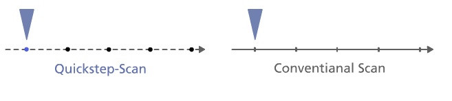
With the implementation of QuickStep Scan, the throughput of the Scanning Capacitance Microscopy (SCM) measurement was dramatically increased, as much as ten times the standard SCM scan speeds, without compromising signal sensitivity, spatial resolution or data accuracy. In QuickStep scan, the XY scanner stops at each pixel point to record the data, and it makes a fast jump between the pixel points.
Introduction
Scanning Capacitance Microscopy (SCM) images spatial variations in capacitance. One of the most common applications of SCM is mapping of the carrier concentration on the non-uniformly doped samples.
In semiconductor manufacturing, the ability to characterize the dopant profile is important in identifying causes of failure as well as in making design advancements.
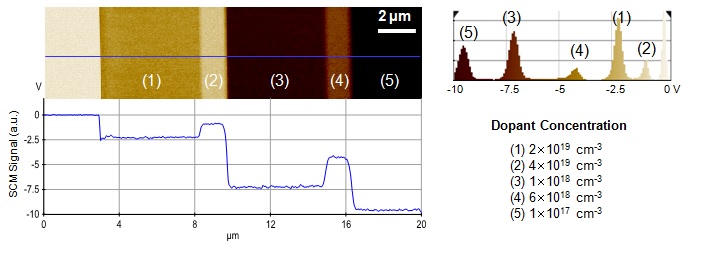
For device characterization, SCM provides the unique ability to measure quantitative 2D dopant profiles.
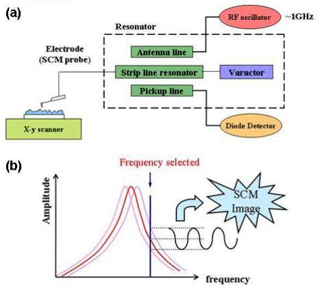
Structure of SCM
The SCM consists of a conductive metal probe tip and a highly sensitive capacitance sensor in addition to the normal Atomic Force Microscopy (AFM) components. Like Electrostatic Force Microscopy (EFM), SCM applies a voltage between the tip and the sample as in Metal-Oxide-Semiconductor (MOS) structures.
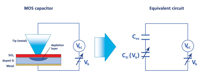
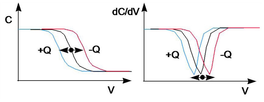
The total capacitance is determined by the oxide thickness and the thickness of depletion layer which depends on the carrier concentration in the silicon substrate and the applied DC voltage between the tip and the semiconductor. The applied AC bias voltage produces capacitance variation at fixed DC bias. The SCM detects differential capacitance (dC/dV) at fixed DC and AC bias voltage as the tip moves across different regions in carrier concentration.
Conventional SCM vs. QuickStep SCM
In order to improve the signal-to-noise ratio, conventional SCM adopts very slow scan speeds as a means of giving the detector enough time to collect data. QuickStep Scan differs from conventional methodology of slow continuous movement. Here, XY scanner stops at each pixel point to record the data and then makes a fast and rapid hop to the next measurement points. This effectively speeds up the scan rate while maintaining the same signal sensitivity of the measurements by conventional SCM at slow scan speeds.
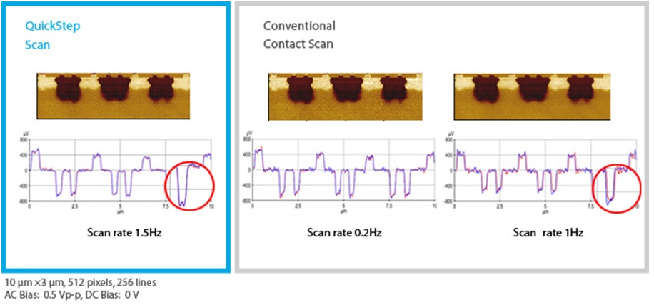
Conventional SCM starts to lose the signal integrity as the scan rate increases, evidenced by the divergence between forward and backward scan signal. The QuickStep SCM maintains the same signal sensitivity as that of slow moving conventional SCM despite scanning at 5~10 times faster scan rates.
In addition, Park SCM is optimized for the best signal-to-noise ratio in the industry by selecting the optimal RF frequency that matches the doping range of sample, over a wide RF band from 600MHz to 2000MHz. From the resonance curve acquired one can maximize the resolution and sensitivity of the SCM probe by choosing the operating frequency which is at the maximum slope.
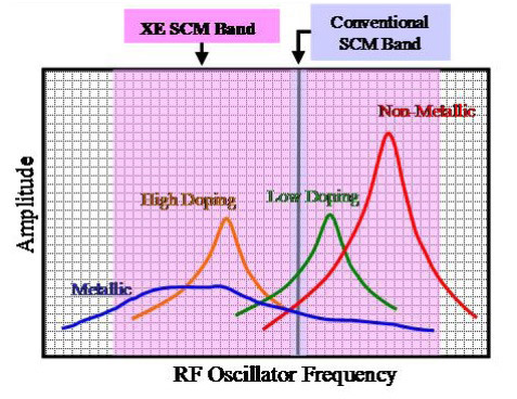
Even when using a very low AC bias voltages, Park SCM detector suppresses noise level and maintains a high signal-to-noise ratio, enough to tell the doping concentration less than an order of magnitude. This helps the semiconductor and device engineers perform failure analysis (FA) more accurately and efficiently with less effort and time.
Conclusion: Results of QuickStep SCM by Park NX AFM Series.
In short, QuickStep SCM is several times faster than conventional SCM, without sacrificing any measurement accuracy. It identifies causes of failure analysis, helps innovate the semiconductor design, and detects dopant concentration difference less than an order of magnitude.