Semiconductor
Wafer defects can’t hide from Park Systems
Atomic Force Microscopy (AFM) leader Park Systems has simplified 300mm silicon wafer defect review by automating the process of obtaining high-resolution 3D images, making it faster and simpler than ever before.
Studying Post-etching Silicon Crystal Defects on 300 mm Wafer by Automatic Defect Review AFM
Ardavan Zandiatashbara*, Patrick A. Taylorb, Byong Kima, Young-kook Yooa, Keibock Leea, Ahjin Joc, Ju Suk Leec, Sang-Joon Choc, and Sang-il Parkc
a Park Systems Inc., 3040 Olcott St., Santa Clara, CA, USA 95054
b SunEdison Semiconductor, St Peters, MO, USA 63376
c Park Systems Corp., KANC 4F, Iui-Dong 906-10, Suwon, Korea 443-270
ABSTRACT
Single crystal silicon wafers are the fundamental elements of semiconductor manufacturing industry. The wafers produced by Czochralski (CZ) process are very high quality single crystalline materials with known defects that are formed during the crystal growth or modified by further processing. While defects can be unfavorable for yield for some manufactured electrical devices, a group of defects like oxide precipitates can have both positive and negative impacts on the final device. The spatial distribution of these defects may be found by scattering techniques. However, due to limitations of scattering (i.e. light wavelength), many crystal defects are either poorly classified or not detected. Therefore a high throughput and accurate characterization of their shape and dimension is essential for reviewing the defects and proper classification. While scanning electron microscopy (SEM) can provide high resolution twodimensional images, atomic force microscopy (AFM) is essential for obtaining three-dimensional information of the defects of interest (DOI) as it is known to provide the highest vertical resolution among all techniques [1]. However AFM's low throughput, limited tip life, and laborious efforts for locating the DOI have been the limitations of this technique for defect review for 300 mm wafers. To address these limitations of AFM, automatic defect review AFM has been introduced recently [2], and is utilized in this work for studying DOI on 300 mm silicon wafer. In this work, we carefully etched a 300 mm silicon wafer with a gaseous acid in a reducing atmosphere at a temperature and for a sufficient duration to decorate and grow the crystal defects to a size capable of being detected as light scattering defects [3]. The etched defects form a shallow structure and their distribution and relative size are inspected by laser light scattering (LLS). However, several groups of defects couldn't be properly sized by the LLS due to the very shallow depth and low light scattering. Likewise, SEM cannot be used effectively for post-inspection defect review and classification of these very shallow types of defects. To verify and obtain accurate shape and three-dimensional information of those defects, automatic defect review AFM (ADR AFM) is utilized for accurate locating and imaging of DOI. In ADR AFM, non-contact mode imaging is used for non-destructive characterization and preserving tip sharpness for data repeatability and reproducibility. Locating DOI and imaging are performed automatically with a throughput of many defects per hour. Topography images of DOI has been collected and compared with SEM images. The ADR AFM has been shown as a non-destructive metrology tool for defect review and obtaining three-dimensional topography information.
Keywords: Atomic force microscopy, defect review, defect classification, defect inspection, non-contact mode, failure analysis, automated AFM, metrology.
1. MOTIVATION
As integrated devices continue to shrink, incoming bare silicon wafer defectivity requirements become more and more stringent. The inspection of bare silicon wafers for surface defects is predominantly accomplished by measuring the difference in laser light scattering (LLS) between the clean surface and a surface defect, where the intensity of the scattered signal is compared to the LLS of a standard latex sphere. The actual surface defectivity can originate from added particles, topological defects, and crystal imperfections. To be able to reduce the number of defects one must know the source of the defect. LLS inspection can only give defectivity counts and a relative size. Therefore, one must rely on defect review techniques such as SEM and AFM to determine the nature and origin of the defects. In this study we focus on very small crystal imperfections which are not easily observed by LLS without some means to make them larger. We have used a decorative etching technique to highlight crystal imperfections to be studied by LLS, SEM, and AFM. The defect analysis can only be accomplished with accurate and reproducible defect coordinate transfer between analysis tools. Here we show how we have successfully and reliably found and characterized the decorated defects by AFM.
2. ADR AFM PROCEDURE
The process in ADR AFM is depicted in figure 1. During this process, the defects of interest are located accurately and imaged non-destructively. Two factors are essential in order to achieve these objectives. First proper linkage between ADR AFM and LLS inspection tool is required to minimize the positioning errors and locate the defects accurately. The linkage for blank wafers is achieved by sample coordinate alignment. Generally there are no alignment markers or fiducials available on blank wafers to be used for alignment. Therefore ADR AFM uses specialized vision to perform the sample alignment properly. Another important factor in AFM defect review is non-contact mode imaging which is required for non-destructive imaging of the samples while preserving AFM tip life such that the tip can last throughout the process for multiple defects.
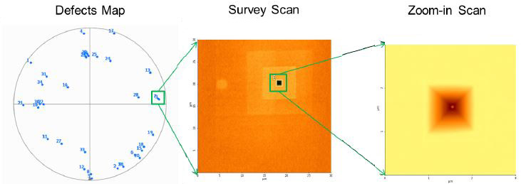 Figure 1.
The schematic shows ADR AFM process for this study. After completing coordinate mapping, ADR AFM will automatically perform survey scan, zoom-in scan, processing, analysis, and classification for each defect.
2.1 Coordinate alignment
Sample coordinate alignment is needed for proper linkage between the stage coordinates of ADR AFM and LLS inspection tool. In the case of blank wafers, no fiducial or alignment marker exists on the sample to be used for sample alignment. To overcome this challenge, a coarse alignment followed by a fine alignment is performed. In the coarse alignment, three randomly selected peripheral and the notch or an angular reference are selected to correct for translational and rotational errors. This is followed by a fine alignment to eliminate positioning errors due to non-affinity between the stage coordinates of ADR AFM and LLS inspection tool. A few large defects with known inspection coordinates are used for performing fine alignment. Since the defects are hardly visible in a standard AFM optical image, an enhanced vision is used to locate the defects in the optics of the ADR AFM and utilize the defects as aligner markers. Upon the sample alignment, ADR AFM is able to locate additional defects accurately. More details on coordinate alignment can be found in ref [2].
2.2 Enhanced vision
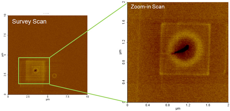
Enhanced vision is utilized during fine coordinate alignment to locate the defects in the optical vision of ADR AFM. The technique is developed based on well-known differential frame averaging of the optical frames collected from the sample surface at two accurately separated locations. The sample can be moved accurately since ADR AFM uses a separated Z and XY scanners configuration. This architecture was initially developed to eliminate the crosstalk between the XY and Z scanners (which has been a common artifact in tube scanner based AFM systems) [2]. In this setup, sample is moved by XY scanner while tip is following the sample topography by Z scanner. In enhanced vision, the optical frames of the sample are collected at two precisely separated locations, and then the final frame is generated from the difference between the collected frames. The resulting frame possesses an enhanced contrast of surface details which are not easily observable in the standard vision of ADR AFM. A comparison between the frames collected by standard vision versus enhanced vision is depicted in figure 2.
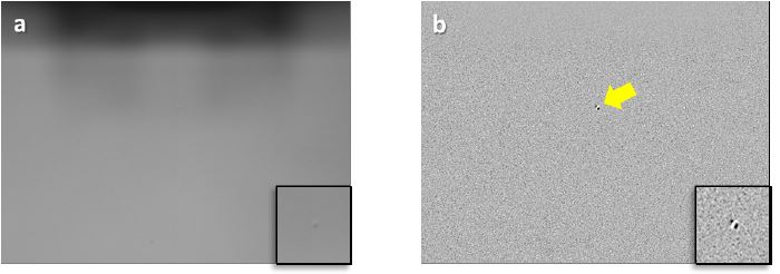 Figure 2.
a) Standard vs. b) enhanced vision images of a small defect on the surface of a bare silicon wafer are shown. The insets show a magnified view of the defect. The small defect is easily observable in enhanced vision. The larger image dimensions are 550 μm × 413 μm.
2.3 Non-contact mode imaging
Non-contact mode is the standard imaging mode in ADR AFM. It is essential to maintain tip sharpness during the defect review process from the first to the last defect that is located and imaged. In addition to keeping tip costs low, wellmaintained tip sharpness ensures consistent image quality and accuracy between the images of all defects during the process. It therefore enables the automated system to uninterruptedly locate and image the defects with a high throughput. In order to perform non-contact mode imaging, the AFM cantilever is oscillated at its resonance frequency. The oscillating cantilever is brought close enough to the sample that the oscillation amplitude reduces to a pre-defined setpoint due to the van der Waals tip sample interaction. ADR AFM maintains the oscillation amplitude to avoid tip contacting the sample. As the tip scans the sample surface, the oscillation amplitude is maintained by moving the cantilever up and down with the Z scanner to maintain its tip sample interaction in attractive regime. More details on non-contact mode imaging can be found in reference [4]. Although ADR AFM's functionality is based on non-contact mode imaging, it is capable of performing in other dynamic or contact imaging modes if needed.
2.4 Automatic defect search and imaging
The significant improvements in throughput of defect review are obtained by ADR AFM due to its fully automated process. Once defect coordinates from LLS inspection tool are entered into ADR AFM, coordinate alignment is performed, the defect is located and imaging starts for the list of selected defects. The process of locating and imaging the defects is fully automated. The automation includes locating the defect, tip-sample engagement, non-contact mode parameter optimization, survey scan, optimizing the scan size, final scan, processing, and defect classification. Defects 4 can be classified into two groups of bumps and pits. Defects are typically located within ±10 μm of their LLS coordinates.
3. SAMPLE PREPARATION (ETCHING PROCESS)
Bare 300mm diameter CZ silicon wafers were treated with a gaseous acid in a reducing atmosphere at a temperature and for a sufficient duration to grow the crystal imperfections [3]. The size and shape of the decorated defects depends on the nature of the original defect as shown in figure 3. Once decorated, the defect size is capable of being detected as LLS event. The LLS inspection tool locates and sizes the LLS events, providing the coordinates to be used by the SEM and AFM.
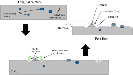 Figure 3.
Schematic of the process used to decorate crystal imperfections for defect inspection.
4. RESULTS
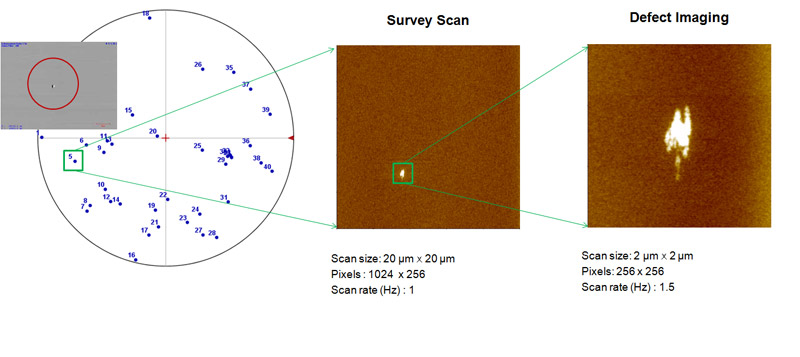
A wafer containing surface decorated defects was inspected by a LLS tool and 34 defects were selected to be reviewed by ADR AFM. The coordinates of the defects were entered to ADR AFM, coordinate alignment performed, and the defects were located and imaged by ADR AFM. The first 21 defects had been imaged by SEM before being studied by ADR AFM. However, SEM images only provide aerial two-dimensional view of defects without sufficient information on the defects depth and out of plane dimensions. The remaining 13 defects were not found by SEM despite the signal collected by the LLS tool. The summarized results of decorated defect study with ADR AFM and comparison with SEM results are demonstrated in figure 4. ADR AFM was able to find all the 34 defects including those that had not been found by SEM.
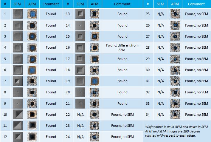 Figure 4.
The results of defect review with ADR AFM and comparison with SEM are shown. ADR AFM was able to locate
and image all the 34 defects.
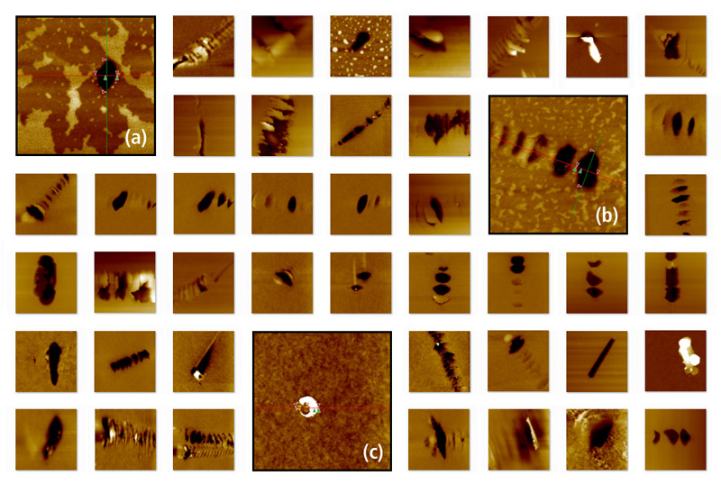
The defects selected to be reviewed by ADR AFM belong to eight types according to their LLS signal. The tentative classification by the LLS tool is based on the defect's light scattering which is dependent on morphology, depth, and presenece of a central defect. As the decorative etching process proceeds, crystal imperfections are exposed and etch at a different rate than the perfect crystal surface. Defects exposed at the initial stages of the etch are deeper and more developed than defects exposed late in the etching proccess. Defects with an inverted pyramid shape are generally deeper and posses higher LLS signal. They are classified as "Facet". Defects with curved shape formed during the late stages of etching are shallower. These defects are classified as "Shallow". Some defects are exposed at an intermediate point in the decorative etch and have some degree of faceted walls with curved bottom. This category is classfied as "Both". Defects which have only started to be decorated have a very weak LLS signal and are classified as "Too shallow". The defects are also categorized whether or not they have the center defect, hence, a total of eight defect types were identified. The defect classification is tabulated in figure 5.
As we go from left to right side of the table in figure 5, the LLS signal become weaker. This was attributed to the depth of defects and the sharpness of the defect's edges. AFM images confirmed the depth difference between different classes of defects. Since the AFM images contain Z heights, we were able to use a banded color scale to depict the surface topography of the defects more accurately in 2D view.
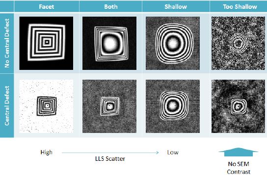 Figure 5.
Defect classification based on the LLS, SEM and AFM data .
5. DISCUSSION
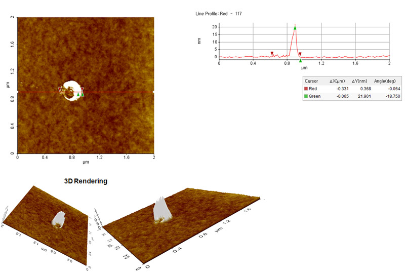
Figure 6 depicts a comparison between the data collected with SEM vs. AFM for the same defect. Primary SEM image provides an aerial 2D view of the defect. However, the shallow depth of the defect reaches the limitations of SEM, hence, poor contrast in the image. As indicated in figure 5, shallower defects were not found by SEM. A secondary electron image helps identify the center defect. Identification of center defect by secondary electron is possible only if the defect was found in primary SEM image.
On the other hand, AFM image not only provides an aerial view of the defect, it also contains the height/depth values for each pixel. Therefore, more information can be obtained about the true topology of the defect by using a 3D representation of the AFM image or using a contoured color scale. Contoured color scales can also help understanding the topology of the defect in aerial view as shown in figure 5. As indicated before, AFM has the highest vertical resolution among all imaging techniques [1], hence, better contrast of AFM images in aerial view.
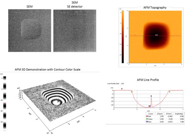 Figure 6.
Comparison between the data collected with SEM versus AFM. SEM image provides an aerial 2D view of the defect. Secondary electron image indicates the presence of center defect. AFM image, in addition to aerial 2D view, includes the 3D data. Therefore a line profile, 3D demonstration, and contoured color scale can be utilized to obtain more information.
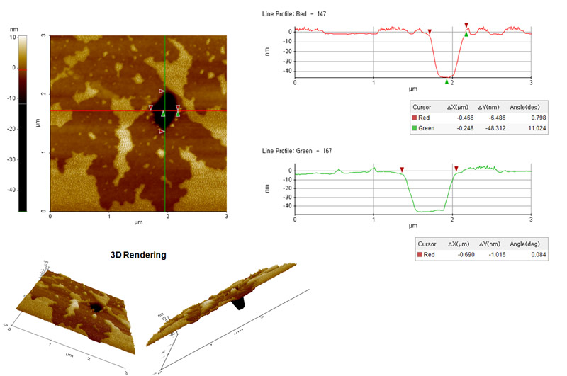
All of the 34 defects were found by ADR AFM including the 13 defects that were not found by SEM. Figure 7 depicts the AFM images a defect that was not found by SEM. The defect depth is below 4 nm and contains a center defect. This example indicates once again the limitation of SEM resolution in out of plane direction.
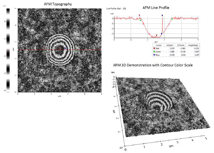 Figure 7.
AFM data for defect #24, which was not found by SEM.
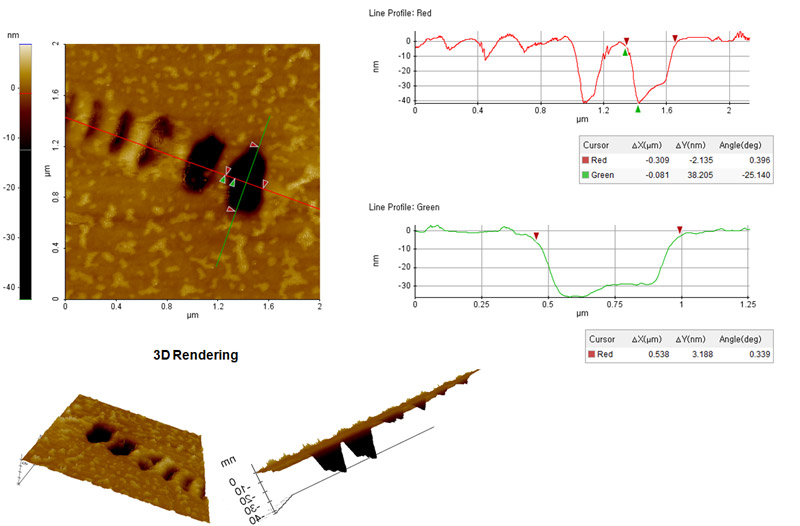
It was indicated above that ADR AFM is a non-destructive imaging technique. It utilizes non-contact mode imaging for survey scan and final imaging scan. However, SEM beam can still modify the sample surface. Figure 8 indicates the sample contamination as a result of electron beam "burning" the surface during SEM imaging. These SEM burn-mark sizes are related to the SEM magnification. Figure 8 shows that several SEM magnifications were used in analyzing this defect.
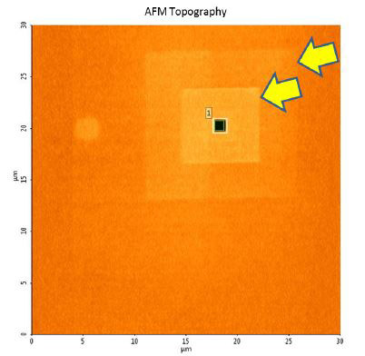
Figure 8.
AFM of a Facet defect with several SEM burn-marks.
6. SUMMARY
We have demonstrated the power of the ADR AFM to provide quality 3D information for defect review on bare silicon wafers. With the automated ADR AFM this type of analysis is simple and yet powerful.
REFERENCES
[1] G. T. Smith, Industrial Metrology: Surfaces and Roundness.: Springer, 2002.
[2] Ardavan Zandiatashbar et al., "High-throughput automatic defect review for 300mm blank wafers with atomic force microscope," in Proc. SPIE 9424, Metrology, Inspection, and Process Control for Microlithography XXIX, 2015, p. 94241X.
[3] J. Libert and L. Fei, Method to Delineate Crystal Related Defects.: PCT Publication, WO2013055368(A1).
[4] Ardavan Zandiatashbar, "Sub-angstrom roughness repeatability with tip-to-tip correlation," NanoScientific, no. Winter, pp. 14-16, 2014.
[5] Ajay Kumar and Banqiue Wu, "Extreme Ultraviolet Lithography: A Review," Journal of Vacuum Science & Technology B, pp. 1743 - 1761, 2007.
[6] James A. Folta, J. Courtney Davidson , Cindy C. Larson, Christopher C. Walton, and Patrick A. Kearney, "Advances in low-defect multilayers for EUVL mask blanks," in Proceedings of SPIE 4688, Emerging Lithographic Technologies VI, 173, 2002.
Sub-Angstrom Roughness Repeatability With Tip-to-tip Correlation

By Ardavan Zandiatashbar, Park Systems Inc., Santa Clara, California.
ABSTRACT
Nano-scale surface roughness measurement has been one of the most common applications of atomic force microscopes over the past two decades. Roughness measurement accuracy and repeatability along with tip life are the major factors that had been considered to be almost impossible to coexist. In this article, we review the basics of non-contact (attractive) mode imaging and introduce soft dynamic mode for special sub-angstrom level roughness measurement applications. The effects of using soft dynamic mode on tip life, measurement consistency and tip-to-tip correlation have been investigated. It is found that soft dynamic mode could be the solution for samples with sub-angstrom surface roughness covered with liquid layer.
INTRODUCTION
Characterization of nano-scale surface roughness and statistical properties of surfaces for different materials is known to be one of the most common applications of scanning probe microscopy (SPM) both in research and production. As an example for SPM application in industrial research and development, surface roughness measurement is required for quality control of glass media samples or heat-assisted magnetic recording (HAMR) products in data storage industry. On the other hand, surface quality control after chemomechanical polishing (CMP) is key factor in determining the reliability of final products in semiconductor production. Nanometer scale roughness of production wafers is important for device patterning in integrated circuit (IC) manufacturing. In all of these applications, understanding the physical property of the sample surface at nano-scale is essential to maintain the reliability and understand failure mechanisms in final products. Atomic force microscopy (AFM) plays a key role in nano-scale surface roughness measurement due to its sub-nanometer level resolution in Z direction. Non-contact (NC) mode or attractive state oscillation imaging has been essential for preserving tip life and consistency in measurements. Although NC mode was the first dynamic force microscopy mode [1], lack of high bandwidth Z-actuator made it difficult to maintain the tip consistently in attractive state. Therefore repulsive state oscillation was used as an alternative which is also known as dynamic mode. Dynamic mode is usually used with high oscillation amplitudes, which leads to limited tip lifetime. Consequently, the data measurement lacks repeatability as it relies heavily on the tip sharpness. Using blunt tips affects significantly the surface roughness measurements as the surface feature size become comparable to or smaller than effective tip radius. Park Systems pioneered manufacturing commercial AFM systems with the focus on performing non-contact mode imaging with high bandwidth Z-actuators and decoupled Z and XY scanners. Here we explain the advances made in AFM imaging for subangstrom surface roughness measurement and repeatability using Park NX system.
DISCUSSIONS NON-CONTACT VS. DYNAMIC MODE
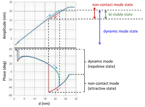
To perform amplitude modulation non-contact mode imaging, the frequency of the cantilever oscillation should be selected slightly larger than the resonance frequency of the cantilever. This frequency selection is based on the fact that the cantilever resonance frequency increases when the cantilever oscillates in attractive state based on the tip-sample separation. In this state, the phase of oscillation for a sharp clean tip is negative in the AFM systems manufactured by Park Systems. (The actual value and sign of the phase signal varies depending on system manufacturer). While Z stage is approaching the sample surface, the cantilever oscillation amplitude is affected by tip-sample interaction forces. This behavior can be observed in Figure 1. In this figure an experimental amplitudedisplacement (A-d) curve is shown. In this curve the oscillation amplitude is measured as the tip approaches towards and then retracts from the sample surface. While the tip-sample separation decreases (red curve), the tipsample interaction is in attractive state (NC mode) until a jump in amplitude occurs and tip-sample interaction transitions to repulsive state (dynamic mode). Similarly when the tip is retracting from the surface (blue curve), it suddenly switches from repulsive to attractive state. As a rule of thumb, this transition generally happens when the tip-sample separation is almost between half to three quarters of free oscillation amplitude of cantilever. This transitional behavior between NC and dynamic modes can be seen as a hysteresis loop in the plot and creates a bistable state [2]. In this state, the feedback system becomes bistable. A corresponding hysteresis loop can be observed in the phase curve as well. In the phase hysteresis loop, phase values transition between negative (attractive state or NC mode) and positive values (repulsive state or dynamic mode).
TIP SHARPNESS BASED ON A-D CURVES
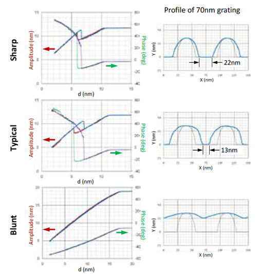
The amplitude curves can be affected by tip sharpness as well. Figure 2 shows three sets of amplitude and phase curves representing sharp, normal, and blunt tips. The tip sharpness is verified by scanning a 70 nm grating. As the tip loses its sharpness, its ability to precisely resolve the gratings becomes limited, while the attractive state region becomes slightly wider. For a normal tip it is easier to maintain the tip in attractive state as this state is wider. For a blunt tip, the amplitude and phase curves do not include the bistable state hysteresis loop, and phase can reach large negative values. In fact, Figure 2 shows that amplitude curve can be used as an estimated tip sharpness/quality characterization tool.
DYNAMIC MODE BENEFITS AND LIMITATIONS
NC mode imaging has the benefits of preserving tip life and measurement consistency, and has been very helpful in measurement of sub-angstrom level roughness values, for example for bare silicon wafers. However, in some cases its performance may be limited when measuring samples with small roughness values (<2Å). In these cases, the image loses resolution and has poor quality. This could be attributed to the presence of liquid layer on top of the sample surface. If the thickness of the liquid layer is comparable to the feature size, it does not allow the tip to track the surface features accurately in attractive state. In order to overcome this issue, tip needs to oscillate in repulsive state. This way it can penetrate the liquid layer and reach the sample surface (contact). This phenomenon is demonstrated by imaging a hard drive glass media sample using both NC and dynamic modes in Figure 3. In this image the sample was initially imaged using the NC mode with the cantilever oscillation amplitude of 10 nm. Despite the acceptable sharpness of the tip, the image quality is not desirable. Sample was imaged again using dynamic mode (with oscillation frequency smaller than the free air resonance frequency (f0)). The dynamic mode image has better quality than the initial image. In the 3rd scan, the sample was imaged in NC mode by using cantilever oscillation frequency larger than f0 and inability of the tip reaching the sample surface was confirmed.
SOFT DYNAMIC MODE
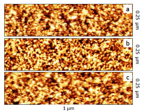
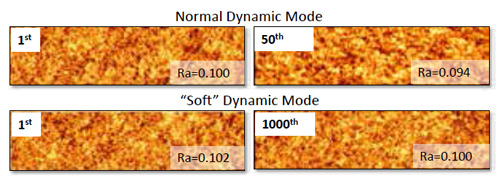
Conventionally dynamic mode imaging is performed with large amplitude oscillation (>20 nm). The larger amplitude oscillation is enabled by applying more energy to the cantilever which facilitates the tip ability to “contact” the sample surface. In addition, the AFM systems ability to perform dynamic mode imaging with low oscillation amplitude was limited due to the bandwidth of the Z servo of the AFM system and system noise level. If a system can perform dynamic mode with low amplitude, it should be able to apply minimum energy to the cantilever, just enough to penetrate the liquid layer, then the tip life may be preserved longer and minimize its effect on the measurement repeatability. Park NX series were designed for low amplitude NC mode imaging, hence it is made possible to perform low amplitude low energy cantilever oscillation with maximum signal to noise ratio. We call this type of dynamic mode (with low oscillation amplitude) soft dynamic (SD) mode. Figure 4 shows a comparison between the tip life in normal dynamic mode (high amplitude) vs. SD mode (low amplitude) by scanning a glass substrate sample with roughness value of about 1Å. In this figure, the 1st and 50th scanned images by normal dynamic mode are compared. The 1um x 0.25um images (512 x 128 pixels) are collected with scan rate of 1Hz. The roughness value (Ra) is decreased by 6% over 50 images and image resolution significantly degrades due to loss of tip sharpness. The two lower images show the comparison between 1st and 1000th images collected with same tip using SD mode. The decrease in roughness value is below 2% over 1000 images, and high image resolution is well-preserved until the last image. Performing SD mode imaging is made possible by using fast Z servo feedback. Despite the gradual tip wear, SD mode clearly outperforms normal dynamic mode in terms of tip life and measurement consistency.
TIP TO TIP VARIATION AND TIP LIFE
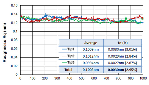
Another important factor about measurement consistency is tip-to-tip correlation. It is desirable to eliminate tip dependency of the measurements in order to obtain true sample surface property by AFM roughness measurement. For this purpose, the 1000-image roughness measurement test was repeated with three different tips. Variations of roughness (Ra) over 1000 scans for the three tips are shown in Figure 5. The average and standard deviation of the data set for each tip is shown in the inset table. It can be seen that for the sample with Ra of 1Å, the repeatability measurements show variations below 0.03Å (below 3%). This minimal variation shows tip independency of roughness measurements using SD mode.
SAMPLE VARIATIONS
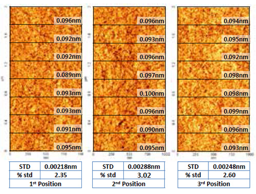
Although the measurement variation is small (<3%), the source of the variation still remains unknown. Figure 6 shows three sets of roughness measurement on different positions on the HDD glass media. At each location, 1um x 2um images with resolution of 512 x 1024 pixels are collected at scan rate of 1Hz in SD mode. Each image is divided to eight 512 x 128 pixel sections in order to be comparable with images collected for Figure 5 and Ra values were measured for each subimage. It turned out that the Ra variation on the sample surface from location to location is around 3% which is comparable to the variation observed in Figure 5. Therefore, one possible source of the 3% variation observed in Figure 5 could be attributed to point to point variation on the sample surface.
CONCLUSION
In this article we introduced SD mode imaging as an alternative method for subangstrom surface roughness measurement by using low amplitude low energy cantilever oscillation with Park NX series. We performed 1000 roughness measurements using one single tip using SD mode and showed less than 3% variation while the image resolution and tip sharpness is preserved. This variation is identical to the variation of roughness over different locations on the sample surface. By repeating the 1000 scan test using two additional tips, significant tip-to-tip correlation with 3% variation was shown to exist. Performing SD mode imaging is made possible by using large bandwidth and high speed feedback system provided on Park NX series. This solution is provided for research and production in different industries including hard drive media and semiconductor manufacturing.
REFERENCES
Automatic Defect Review AFM with Enhanced Vision
 By Dr. Ardavan Zandiatashbar, Ph.D.,
Research Scientist Park Systems Inc., Santa Clara, California.
ESSENTIAL TOOL FOR HARD DISK MEDIA FAILURE ANALYSIS
Failure analysis engineers in data storage rely on atomic force microscope (AFM) as one of the key techniques for obtaining threedimensional information about the topological defects on hard disk media samples. This information is critical for proper identification of defects and eliminating defect sources. Although optical microscopy can provide a quick image of sample surface, the technique has limited resolution due to light wavelength. On the other hand, electron microscopy can provide higher resolution but it is essentially a destructive technique and provides only a twodimensional image. AFM provides the highest vertical and lateral resolution and provides a three-dimensional topography of the sample surface [1]. The conventional AFMs were known to have limited throughput and tip life since imaging was performed in destructive mode. To address these limitations of AFM, Park Automatic Defect Review (ADR) AFM has been developed and introduced in mid 2000s for a non-destructive high throughput 3D imaging of defects. This solution was widely accepted and welcomed in failure analysis (FA) labs globally. In this article we introduce the latest generation of ADR-AFM. The new ADR-AFM utilizes enhanced vision technique to facilitate locating defect of interest (DOI). This solution carries the commercial name of Park NX-HDM.
The main objective of the FA lab for hard disk media is studying the defects and investigating the possible defect sources to improve yield management. For this purpose, defect study consists of two main steps: defect inspection, and defect review. In defect inspection, an inspection tool searches the media surface using optical, electron beam, or magnetic probe to find the location of the defects. The output is a map of defects which indicates their distribution over the sample surface. The defect map can also be used for locating the DOI for further investigation. Although the inspection tools have high throughput and are able to test several samples per hour, they are limited in resolution and are not suitable for characterizing each defect effectively. Therefore some of defects are selected for defect review and detailed characterization. In defect review, defects of interest are characterized to obtain a high resolution image and classified accurately. The defect review process relies on techniques that can provide high resolution topographical information about each defect. The examples for defect review techniques are AFM and S/TEM. Unlike inspection tools, the review techniques are relatively slower and need to accurately locate DOI for imaging.
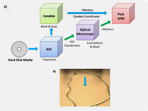 Figure 1.
a) Current process of defect inspection and review for hard disk media. The green path shows the process path for conventional AFMs. The blue path shows the process with the first generation of Park ADR-AFM.
b) A defect on hard disk media sample which is marked by a surrounding scratch. The defect is hardly visible in optical vision of AFM.
Locating DOI is the major challenge for defect review tools. There is a difference between the coordinates of DOI on the stage of inspection tool versus its coordinates on the stage of review tool. This difference is referred to as stage error. The stage error is generally larger for in-house inspection tools (e.g. AOI, Tester) comparing to commercial inspection tools (e.g. KLA-Tencor Candela). The process of defect inspection and review is depicted schematically in Figure 1a. In the past and before introducing ADR-AFM, manual AFM was used for imaging DOI. To facilitate locating DOI in manual AFM, FA engineers initially marked every single defect. As shown in Figure 1a hard disk media is inspected with an automated optical inspection (AOI) tool which is the most commonly used equipment in mass production and the map of defects is generated. Then the disk is investigated by an optical microscope for locating and marking each DOI. Marking defects was done by making observable scratches around each defect to facilitate finding it through the optics of AFM (Figure 1b). This process path is shown by green arrows in Figure 1a. This included performing multiple survey scans to find DOI. This method had a low throughput of 10 defects per day in best scenario. In addition, conventional AFMs were using destructive scanning method (tapping mode), therefore, tip life was limited due to performing multiple large survey scans that was required for finding each defect and the whole process resulted in high cost of ownership.
The first generation of Park ADR-AFM had been introduced in order to address the limitations of conventional AFMs in the defect study process. This solution provided two major advancements comparing to conventional AFMs. First, it has a significantly improved throughput up to 10 defects per hour as a result of automated process. Since the system was operated by automated software, the user did not need to be present during the scan. Hence the system could continue locating and imaging a large number of defects on its own (even overnight). This improved the throughput of an AFM system significantly. Second, the imaging was performed in non-contact mode. Using non-contact mode imaging extended the tip life, which is critical for automated defect review process and getting consistent data. Therefore a single tip could be used for a significant number of images without user being present.
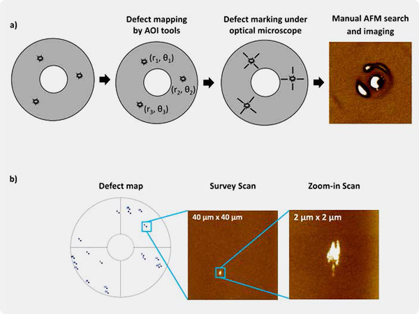 Figure 2.
The AFM based defect study process is schematically shown for a) manual AFM, b) ADR-AFM. In ADR-AFM, locating the defect from defect map, survey scan, final zoom-in scan are performed automatically by the system.
The ADR-AFM process is depicted in Figure 2 and compared to conventional process using manual AFM. In conventional AFM imaging (Figure 2a), the sample surface was first searched with an inspection tool. This was followed by marking the DOI on the surface using optical microscope. After laborious efforts of marking each DOI, the sample was brought to AFM for imaging. Finding the defect in AFM required visual search in vision and followed by multiple low and high magnification scans (green path in Figure 1a). In ADR-AFM, DOI coordinates from inspection tool are initially imported which is followed by coordinate alignment. After this step, automated software moves the tip to each defect, performs a survey scan, images the defect, and classifies the defect automatically. With ADR AFM throughput of defect review increases up to 100 defects per day. In addition, since this process is fully automated, engineer do not need to stand by and operate the system during the runs which frees up their time and boosts productivity.
The survey scan size of old Park ADR-AFM was selected based on the stage error of the inspection tool used to generate defect maps. A 40 μm × 40 μm survey scan was typical to cover for a stage error up to 20 μm between AFM and Candela. Since the stage error of AOI tools are very large (≥ 50 μm), using a linkage tool (e.g. Candela) with smaller stager error was necessary in order to have the process of defect study complete as shown by blue path in Figure 1a. A set of 16 markers were added to each wafer before the inspection run by Candela to be used for sample alignment in Park ADR-AFM.
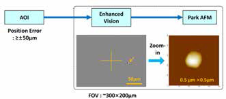 Figure 3.
An example of enhanced vision image and how it facilitates linkage between the AOI tool which has larger stage errors and Park ADR-AFM.
The new generation of Park ADR-AFM is introduced recently for both hard disk media and 300 mm wafers [2]. Bright field enhanced vision is introduced in the new generation of Park ADR-AFM. It provides the ability to observe defects in ADR-AFM optical field of view (FOV). Bright field enhanced vision utilizes differential frame averaging technique and precise movement of sample by decoupled XY scanner to observe small defects that are hardly visible through regular optics of the system. Decoupled XY and Z scanner structure of Park ADR-AFM enables using differential frame averaging by collecting optical images of the sample surface at two precisely separated positions of XY scanner. The differential image of the frames of sample surface collected at two different positions enhances the contrast of small defects and makes them visible in optics of ADR-AFM. Since the FOV of ADR-AFM is larger than the maximum survey scan size, enhanced vision enables the ADR-AFM to accommodate even larger stage errors of inspection tools (Figure 3). Collecting a typical bright field enhanced vision image takes between 1 – 30 sec for each defect.
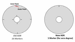 Figure 4.
The schematic shows the sample alignment process in the first (left) versus the new (right) generation of Park ADR-AFM. In the latest Park ADR-AFM only one marker is needed to indicate zero-degree location of hard disk media samples.
In addition to bright field enhanced vision, a new sample alignment algorithm is developed to facilitate the linkage between the ADR-AFM and inspection tools. In the first generation of ADR-AFM, a sample alignment by using 16 markers was needed to align the sample on the ADR-AFM stage. The coordinates of 16 markers were generated by Candela, and were matched with the coordinates of ADR-AFM stage. In the next generation of ADR-AFM, only one marker is needed for sample alignment. The new alignment process consists of one coarse and one fine alignment step. In the coarse alignment, three points at the circular perimeter of the hard disk media sample is used for finding the sample center, and a zero-degree marker is used for finding the rotation of the sample. In the fine alignment step, ADR-AFM uses few larger defects for minimizing the remaining positioning errors by utilizing enhanced vision. The new alignment process is faster and more convenient for sample alignment comparing to the first generation of ADRAFM. In addition, it can also be used as a tool for evaluating the stage error of AOI or other inspection tools (Figure 4).
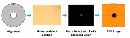 Figure 5.
The new ADR-AFM process with newly introduced dark field enhanced vision for hard disk media with reflective surface.
Dark field enhanced vision is introduced in the latest generation of Park ADR-AFM. The new dark field enhanced vision enables AFM to observe defects in a short time on reflective surfaces by collecting the light scattered due to surface defects. For this purpose, a new hardware module is developed and implemented in the AFM system. In this module a laser beam is emitted to the location of interest on the sample. The beam angle of incidence is larger than zero degrees such that the direct beam reflection is not collected by the on-axis optics of ADR-AFM. For a reflective sample, majority of laser beam is following the expected reflection path with similar angle of incidence. In case the surface a topological defect is present on the sample surface, part of the laser beam will be scattered in different directions other than the regular reflection path and are collected by on-axis ADR-AFM optics. The collected frame is an image of the surface with collected scattered light from the defects. Examples of standard optical and dark field enhanced vision images are shown in Figure 5. The upgraded ADR-AFM process with dark field enhanced vision is presented schematically in Figure 5. In the new process, after the sample alignment, ADR-AFM goes to defect location, recognizes the defect using dark field enhanced vision (without AFM scanning), and performs the imaging, analysis, and classification. The new process enables ADR-AFM to minimize the positioning error. As a result the required survey scan is also minimized and the throughput is increased. As a result, it enables ADR-AFM to accommodate defect maps from AOI systems that have large stage errors. The ability to see the defects by enhanced vision enables ADR-AFM to be used as the reference tool for evaluating the stage errors of different inspection tools.
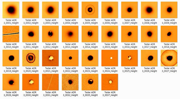 Figure 6.
The results of performing ADR-AFM on a 95 mm hard disk media samples for a set of defects reported by an in-house inspection tool. 33 defects out of 37 was found and imaged by ADR-AFM.
The results of a defect review by ADR-AFM on a 95 mm hard disk media sample are shown in Figure 6. The defect coordinates were provided by an in-house inspection tool with large stage error (> 50 μm). Dark field enhanced vision has been used for locating the defects. As the result, ADR-AFM was able to find 33 out of 37 defects successfully using the addition of enhanced vision. The defects are classified to two groups of pit and bump by ADR-AFM. An example of each group is depicted in Figure 7. In this figure dark field enhanced vision images and AFM images of defects are shown. ADR-AFM was able to find defects with vertical dimension as low as < 3nm.
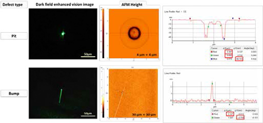 Figure 7.
Representative pit and bump type defects on a hard disk media samples which were found and imaged by ADR-AFM. The dark field enhanced vision images are shown side by side the AFM images and selected profiles of the defects.
In summary, the latest generation of Park ADR-AFM is equipped with new bright field and dark field enhanced vision modules. The bright field enhanced vision utilizes frame averaging technique and ADR-AFM’s decoupled XY scanner to obtain a high resolution optical image of the sample surface to help locating the DOI. Dark field enhanced vision is enabled by collecting the scattered laser signal by the on-axis vision of ADR-AFM and enables detecting defects on the surface of reflective surfaces. Park ADRAFM uses non-contact mode imaging and therefore is imaging the samples in a non-destructive method. Park ADRAFM with enhanced vision modules and updated alignment algorithms is used for high throughput AFM based defect review. Additionally, ADR-AFM with enhanced vision is a potential reference tool for evaluating the stage error for inhouse inspection systems that are being developed or maintained.
REFERENCES
[1] Smith, G. T., Industrial Metrology: Surfaces and Roundness, Springer, London, 103-105 (2002).
[2] Ardavan Zandiatashbar et al., "Highthroughput automatic defect review for 300mm blank wafers with atomic force microscope," in Proc. SPIE 9424, Metrology, Inspection, and Process Control for Microlithography XXIX, 2015, p. 94241X.
Automated AFM Significantly Boosts Throughput in Automatic Defect Review
Reduces Cost and Increases Efficiency in Production of Semiconductor Wafers
Introduction
The scaling trend in semiconductor design requires tighter control over defects on wafers. In order to characterize the defects, both inspection and review tools are needed.
The inspection tools such as surface scanning inspection systems (SSIS) are employed first to locate and map defect sites, and the review tools such as scanning electron microscopy (SEM) are used to obtain morphological information.
Large defects, which are visible by optical microscopy, can be easily found by an inspection tool and imaged by a review tool. However, as processing requirements become more stringent, the defect size of interest gets smaller, below the diffraction limit of optical microscopy. To locate and identify small defects, a large survey scan needs to be performed by the review tool in order to find the exact location of the defects.
Defect review SEM has been used to image the defects of a bare wafer after defect sites are mapped by the laser-scattering defect inspection tools such as Surfscan from KLATencor. However, the imaging by defect review SEM is limited to 2D and cannot provide the 3D information, which has become more crucial in recent days for bare wafer manufacturing control. Also, smaller defects, less than 50nm, are increasingly not detected by defect review SEM.
Why Automatic Defect Review (ADR) AFM?
Atomic force microscopy (AFM) is gaining more importance as the choice of a review tool in recent days because it can directly measure the defect dimensions (height and width, hence shape) and the physical properties of defects of interest. However, for engineers and researchers working with bare wafers, the process of identifying nanoscale defects is time consuming with conventional manual AFM, hindering productivity, let alone throughput. Thus it is important to have an automated solution for both failure analysis and production engineers who need to find the cause of defect sites on bare wafers and minimize them.
To address this need, Park Systems have delivered the Automatic Defect Review (ADR) AFM which speeds up and improves the way defects are imaged and analyzed. With this solution, users are now able to obtain the additional details and the height/depth information of the defects which were not possible or too expensive to obtain with SEM based ADR.
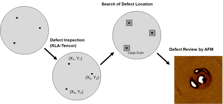
How to Transfer Defect Map from Inspection Tool to Review AFM
The general defect review concept is simple, yet complicated when it is done on the nanometer scale. Simple, because all it would require is the proper transferring of the defect map from an inspection tool and re-locating those same defects on a review tool. Coordinates from the inspection tool are translated to the review tool, which is used to zoom in and image the details of the defect, revealing its characteristics.
The complicated part comes into play when attempting to accurately go near the defect site, in order to image it, and to do this all in automation. This is due to the fact that there are stage mapping errors between the inspection tool and the review tool.
In case of a patterned wafer, alignment marks are used as reference points to map the two stages between the inspection tool and AFM, and the position error from both tools can be accurately estimated. Park’s initial success in Automated Defect Review (ADR) AFM solution was implemented in the hard disk industry, utilizing the reference marks inscribed by the optical inspection tool such as KLA Tencor’s Candela series. Utilizing these marks, the defect maps of hard disk media or substrates could be accurately and reliably transferred and the automated review AFM, Park HDM Series, was able to get near enough to the defect to conduct a survey scan, and then follow up with a zoom-in scan to provide the details the user required. As a whole, this solution proved to be effective, increasing the productivity in the HDD industry’s FA labs by up to 1000%.
Automated, Accurate Transfer of Defect Map WITHOUT Reference Marks
Success in the HDD industry resulted in similar requests coming from the semiconductor industry. Since the cleanness level requirement for the semiconductor industry is much stricter than that of HDD, creating markers on the bare wafers is not possible, hence the need for ADR process WITHOUT any reference marking on a bare wafer is required.
Without alignment marks the positions of defects are roughly estimated [1, 2]. Therefore, additional alignment process is required to decrease the positional error [3] during the defect map transfer. To address this issue, a new method was developed that utilizes the wafer edge, notch, and large defects, which are visible by optical microscopy, as the reference points.
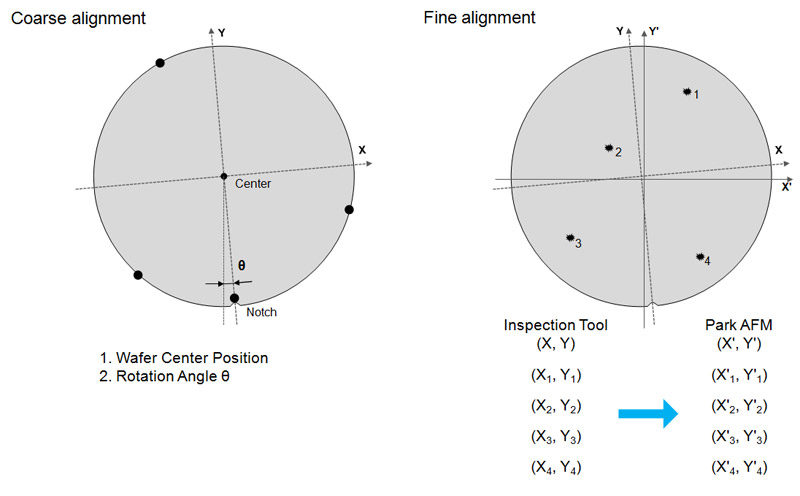
The improved remapping technique, combined with enhanced vision, does not require any reference marker on a bare wafer. Furthermore, it also does not need any separate step to calibrate the stage of the targeted inspection system.
The success rate of the 300mm bare wafer ADR depends on two factors: the accuracy of stage mapping and the size of initial survey scan. The more accurate the stage mapping, the smaller survey scan size can be used for higher success in finding the defect. The new stage mapping technique vastly improves the accuracy by adopting advanced remapping algorithm and enhanced vision technique.
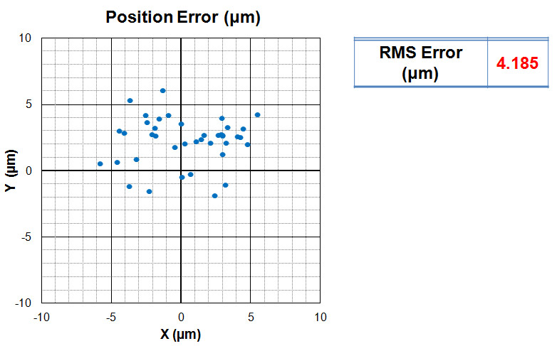
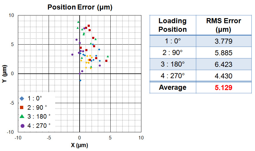
The RMS position error of survey scans are less than 5 μm regardless of wafer loading positions. It means that all the defects are located within ±5 μm using the defect map provided from a defect inspection tool.
Conclusion: Results of 300 mm Bare Wafers ADR by Park NX-Wafer
Utilizing the advanced coordinate translation technique, the defect map obtained from a laser-scattering defect inspection tool, such as Surfscan from KLA-Tencor, can be accurately transferred to a 300mm AFM system, allowing full automation for high throughput defect imaging.
With the new 300mm bare wafer ADR, a typical automated measurement run would go as follows.
- A bare wafer is run by a laser-scattering defect inspection tool (e.g. Surfscan)
- Then an operator registers the resulting defect coordinates file, known as KLARF for the Surfscan tool, to Park NX-Wafer.
- The coordinates of the defect map are automatically de-skewed and the linkage of the two stages is enabled between the inspection tool and Park NX-Wafer
- Park NX-Wafer then runs the automatic defect review (ADR) on the sample bare wafer.
The above set of data shows the results from the 300mm bare wafer ADR with Park NX-Wafer. Typical success rate is higher than 95% regardless of the orientation of a wafer. The zoomed-in scans show the detailed morphology of defects, clearly distinguishing various types such as pit, bump, and scratch.