Manufacturing Review
Semiconductor-based device fabrication and microelectromechanical systems (MEMS) technology have been major sources of the great success enjoyed by the modern high-tech manufacturing industry. Semiconductor-based device fabrication produces logic and vertical memory devices (fin structure, STI, TSV), liquid crystal displays (LCD), light-emitting diodes (LED), organic LED (OLED), and contact image sensors (CIS), etc. MEMS structures provide various photonic applications including the production of wave guide structures. In those industrial device manufacturing processes utilizing both semiconductor-based and MEMS techniques, reviewing (inspection) the correct dimension of device structures and any unintended defects on on them is critical to maximize productivity and cost-efficiency at every step of the whole in-line process.
Recently, as the size of both device structure and defect becomes smaller, down to the range that optical inspection techniques are unable to detect, the need to review at higher and higher sensitivity has been increasing in the manufacturing industries. This has resulted in the adoption of techniques capable of nanometer resolution review such as atomic force microscopy (AFM).
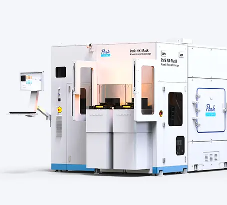
Many industrial researchers and engineers choose Park Automated AFM for their review of aspects of structural geometry such as feature height, pitch, critical dimension (CD), angle, and even sidewalls together with roughness analyses. This is due to their awareness of Park Automated AFM's accurate measurement results, low system noise, high-throughput rate, and minimized tip-to-tip variation from True Non-Contact™ mode AFM imaging technology.
Featured Products
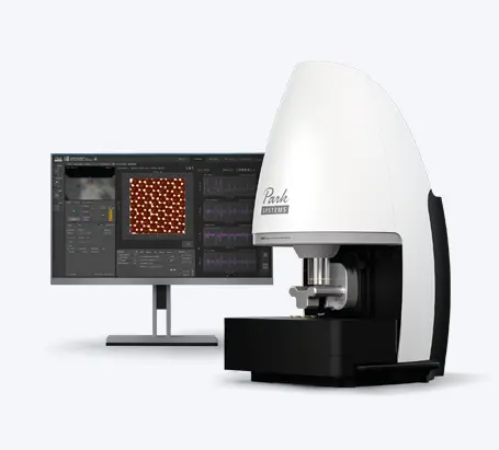
Park Systems is dedicated not just to advancing research, but industry as well. That’s why our designers have worked to build a line of the most effective AFMs for FA engineers and industrial applications. Allowing users to take highly accurate measurements and complete their work more quickly, these tools can improve efficiency in the workplace and reduce errors, leading to a more profitable, more consistent development and production process.
Park NX-Wafer
The Park NX-Wafer is the only wafer fabrication AFM with automatic defect review. This gives it the power to increase the throughput of your lab by up to 1000% while ensuring a high level of accuracy and quality control when scanning wafers up to 300 mm in size.
Park NX-3DM
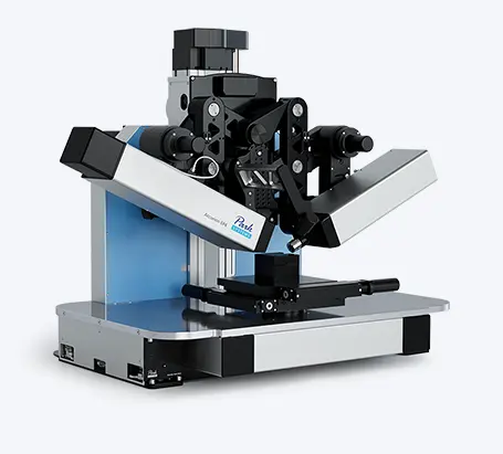
Park NX-3DM is the completely automated AFM system designed for overhang profiles, high-resolution sidewall imaging, and critical angle measurements. With the decoupled XY and Z scanning system with tilted Z-scanner, it overcomes the challenges of the normal and flare tip methods in accurate sidewall analysis. In utilizing our True Non-Contact Mode™, the Park NX-3DM enables non-destructive measurement of soft photoresist surfaces with high aspect ratio tips.
Park NX-PTR
The Park NX-PTR is a fully automatic industrial in-line AFM solution for, but not limited to, automatic pole tip recession measurements on rowbar-level, individual slider-level, and HGA-level sliders. With sub-nanoscale accuracy, high repeatability and throughput, the Park NX-PTR is the metrology tool of choice for Slider manufacturers to improve their overall production yield.
Technical Notes
Semiconductor
- Automatic Defect Review (ADR) of 300mm Bare Wafers with Automated AFM
- High Throughput and Non-Destructive Sidewall Roughness Measurement Using 3-Dimensional AFM
- New 3D-AFM for High Resolution Sidewall Imaging