Myung-Hoon (Brian) Choi,1 Hanaul Noh,1 Jason Hsieh,1 Ashton Enrriques,1 Gilbert Min,1
Jake Kim,2 Xingchen Ye,3 Lane A. Baker4 and Stefan Kaemmer1
1Park Systems Inc., Santa Clara, CA, USA 2OBU, Park Systems South Korea
3Department of Chemistry, Indiana University in Bloomington, IN, USA
4Department of Chemistry, Texas A&M University, TX, USA
Abstract:
Cetyltrimethylammonium bromide (CTAB) is a widely used surfactant in the aqueous synthesis of colloidal nanoparticles, but residual CTAB on nanoparticle surfaces can affect performance in applications such as catalysis and sensing, particularly under hydrated conditions. To gain a fundamental understanding of CTAB adsorption, we employed a colocalized measurement approach that combines in situ atomic force microscopy (AFM) with scanning electron microscopy (SEM). Using a nanoscale cubic model system, we correlatively analyzed AFM and SEM data to characterize CTAB adsorption on the top surface of individual gold nanocubes (Au NCs) with high precision. This approach enabled statistical determination of the CTAB layer thickness at the single-nanocube level. The mean thickness of the CTAB adsorption layer was measured to be 2.9 ± 2.4 nm, equivalent to the theoretical length of a single CTAB molecule (~2.2 nm). Our correlative AFM–SEM analysis demonstrates that in situ AFM is a powerful and broadly applicable tool for evaluating ligand presence and removal on nanomaterials under their operational, hydrated state.
Key words: CTAB, Gold Nanocube (Au NC), In situ AFM, Correlative AFM-SEM Measurement
Introduction
Gold nanoparticles have long attracted research interest due to their unique physicochemical properties and diverse applications in biomedicine, catalysis, and sensing.1 Historically, these applications were primarily enabled by simple spherical nanoparticles, which offered limited control over surface structure and functionality.2 The development of colloidal nanocrystals with precisely controlled shapes and sizes - particularly through seed-mediated synthesis - has opened new possibilities for tuning properties and expanding the functional scope of gold-based nanomaterials.3,4 A key factor in achieving such morphological control is the role of surface ligands, which direct nanocrystal growth by selectively binding to specific crystallographic facets and modulating surface energies. Among these, cetyltrimethylammonium bromide (CTAB) has emerged as a crucial surfactant and shape-directing agent in the synthesis of anisotropic gold nanocrystals, such as nanorods and bipyramids. Understanding how CTAB adsorbs and organizes on nanocrystal surfaces is essential, as its presence influences not only the growth process but also the resulting surface chemistry, reactivity, and performance in advanced applications. For instance, residual CTAB can impact electrocatalytic activity by altering charge transfer and interfacial accessibility.5 Ensemble techniques such as spectroscopy and light scattering have suggested the formation of a ~32 Å thick CTAB bilayer on gold nanorods, but lack the spatial resolution to resolve its arrangement at the single-particle level.6 As the field advances toward highly tailored nanocrystals with shape-dependent functionality, detailed insights into ligand adsorption are increasingly critical for optimizing synthesis and enhancing performance across application domains.
We investigated the heterogeneity in the distribution of CTAB on the surface of gold nanocube(Au NC) at the nanoscale by leveraging the complementary strengths of atomic force microscopy (AFM) and scanning electron microscopy (SEM). AFM excels at capturing vertical (height) information with sub-nanometer precision and is capable of measuringin liquid environments where the surfactant layers remain hydrated which is key for understanding the initial adsorption state. In contrast, SEM provides high lateral resolution (width and length) imaging under vacuum. By combining these two techniques, we developed a correlative microscopy approach that enables accurate three-dimensional (3D) characterization of individual Au NCs and effectively visualizes the distribution of the top surface-bound ligands.
Experimental
Metallic Nanocrystal: Gold NanoCube
Figure 1b presents a schematic diagram illustrating the seed-mediated growth mechanism.3 In this process, the shape of the nanocrystals is controlled by the relative growth rates of different crystallographic facets. Specifically, the ratio (R) of the growth rates of the {100} facets to the {111} facets (R = {100}/{111}) determines the resulting morphology of the nanocrystals. When the growth rate of the {111} facets is slower than that of the {100} facets (i.e., R > 1), the {111} facets become more prominent, resulting in shapes such as octahedra. Conversely, when the {100} facets grow more slowly than the {111} facets (R < 1), the {100} facets dominate, leading to the formation of nanocubes. By carefully tuning the reaction conditions, such as the concentration of growth precursors, surfactants, temperature, and reaction time, the growth rates of these facets can be controlled to favor the formation of specific shapes. This precise control over morphology is critical because the shape and exposed facets of nanocrystals significantly influence their physical, chemical, and catalytic properties. Therefore, understanding and manipulating facet-specific growth rates is fundamental to tailoring nanocrystals for targeted applications.
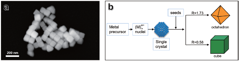
Figure 1. Scanning electron micrograph of a gold (Au) nanocube with {100} FCC (face-centered cubic) facets (a) SEM image is showing a gold nanocube with well-defined {100} facets, which were synthesized using the seed-mediated nanocrystal synthesis method. (b) Diagram illustrating the mechanism of the seed-mediated method, which highlights the ratio (R) between the growth rates of {100} and {111} facets (R: {100}/{111}).
In Situ AFM Set-up
The liquid holder shown in Figure 2a is designed for high-resolution in situ AFM imaging of biological and biochemical materials, allowing these samples to maintain their native properties under hydrated conditions. It also isolates the electrical components of the AFM probe holder from the liquid environment, reducing the risk of short circuits. This optimized design ensures precise beam alignment by minimizing the refractive index differences at the air–liquid interface. The probe holder, constructed from polyether ether ketone (PEEK), offers excellent chemical resistance, including acids. A round silicone cover (Figure 2b) can also be fitted to create a sealed
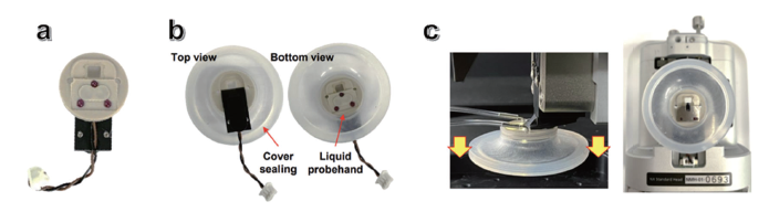
Figure 2. Images of the components used for in situ AFM imaging: (a) Liquid probe holder (LPH), (b) LPH with sealing cover attached, and (c) LPH with sealing cover installed in the AFM head.
liquid environment, enabling stable and controlled in situ AFM imaging. Figure 2c illustrates the complete in situ AFM imaging setup, including the AFM head and sample stage. The topography of Au NCs in H2O was obtained by AFM (NX12 platform). Prior to topography acquisition, piezoelectric scanners were calibrated with a standard sample, TGQ1. Au NC samples were imaged in H2O, in a liquid cell sealed by a silicon cover to prevent evaporation and reduce thermal drift (Figure 2b). Soft tapping mode was conducted in situ with an amplitude of 5−10 nm at 25−30 kHz resonance frequency. The softness (spring constant: 0.1 N/m) of the cantilever (USC-F0.3-k0.3, NanoAndMore) and small dimension of the cantilever (length 38 μm and width 16 μm) and tip (ca. 10 nm radius) used here provide sufficient sensitivity for imaging in hydrated conditions with high topographical resolution.7-9 Data analysis was carried out by using SmartAnalysis, XEI software (Park Systems)10-12
Sample Position Linkage System for Correlative AFM and SEM
Accurately locating the same nanocrystal for sequential AFM and SEM measurements is a critical step for effective correlative analysis. However, differences in sample stage dimensions and orientations between AFM and SEM systems often make it time-consuming and challenging to identify the same location across both instruments.
At the nanoscale, even minor mismatches in orientation or magnification, especially during SEM operation, can result in the loss of the region of interest, making correlative imaging particularly challenging.
This challenge is effectively addressed by the sample position linkage system provided by Park Systems (Figure 3). The custom sample holder, shown in Figure 3a, features three reference markers located at the edges, each with a distinct circular pattern (Figure 3b) that are easily identifiable in both Park AFM and JEOL SEM systems. The software automatically detects these markers and generates precise XY coordinates across the entire sample stage. To integrate the linkage sample holder with the AFM’s XY stage, an additional adaptor is used (Figure 3c). This setup enables seamless, accurate navigation between AFM and SEM, significantly enhancing the efficiency and reliability of correlative nanoscopic imaging.
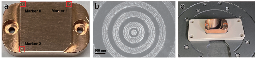
Figure 3. Sample position linkage system for AFM and SEM. (a) Sample holder featuring three fiducial markers (red squares). (b) SEM micrograph displaying the marker pattern used for affine transformation. (c) Linkage sample holder assembled on XY sample scanner of Park AFM
Sample Transfer Shuttle for Air-Sensitive Sample
AFM imaging under vacuum or inert conditions represents another important form of in situ AFM, particularly for studying air-sensitive materials. Figure 4a shows a sample transfer shuttle (Nanoserv Pte Ltd, Singapore) specifically designed to enable the transfer of samples prepared in an inert environment, such as inside a glovebox, without exposure to ambient air. This sealed transfer process is essential for preserving surface integrity and preventing oxidation or contamination.
When combined with an AFM stage adapter, samples can easily be transferred to AFMs operating in controlled environments (Figure 4b), high-vacuum AFM systems (Figure 4c), or SEM instruments. While the shuttle provides XY localization within a limited range of the circular range of the sample holder, it enables safe and efficient transfer of ambient-sensitive samples across different instruments, supporting reliable, high-resolution measurements under vacuum or inert conditions.
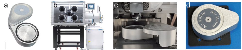
Figure 4. AFM setup for ambient-sensitive sample. (a) Sample transfer shuttle in an open state. (b) a photograph showing Park AFM equipped in a glovebox. (c) an example of AFM measurement where an air-sensitive sample prepared in a glovebox and transferred for AFM measurement. (d) Sample transfer shuttle assembled on an adopter of XY sample stage, ready for transferring to high vacuum AFM or SEM measurements.
Scanning Electron Microscopy
SEM images were obtained on an Auriga FIB-SEM microscope equipped with in-lens and Everhart−Thornley detectors at 20 kV of electron high tension , 30 μm of aperture size, and 5.7−6.0 mm of working distance. Samples were sputter-coated with a conductive Au/Pd layer to mitigate charging during SEM imaging. Line profile analysis of electron micrographs was performed with ImageJ (NIH).13
Results and Discussion
Colocalized AFM and SEM Measurement Steps
In situ AFM topography of individual nanocrystals was first acquired in the presence of deionized water. After imaging, the sample was fully dried under ambient conditions for one hour. To enable high-resolution SEM imaging, a thin metal coating was then applied to the dried sample. The overall procedure is illustrated in Figure 5. All nanocrystals were deposited onto a glassy carbon substrate, with a layer of CTAB surfactant remaining adsorbed on the surface.
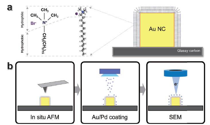
Figure 5. Experimental steps of colocalized in situ AFM and SEM measurements for single nanocrystal analysis. (a) Molecular composition (left) and structure (center) of CTAB, adsorbed to the surface of the Au NC (right). (b) Schematic illustration of the sequential steps involved in the in situ AFM and SEM measurements. The process begins with the in situ AFM measurement, followed by the deposition of an Au/Pd coating on the surface of the nanocubes for subsequent SEM analysis. The length of CTAB molecule estimated in Avogadro software was 21.7 Å.
In situ AFM measurements
The morphology of Au NCs with adsorbed surfactant was examined with in situ AFM under hydrated conditions. One example of the obtained topography is shown in Figure 6a. Measured AFM topography includes the CTAB layer on the top surface and the side wall. Topographies of four single Au NCs were obtained under the same imaging conditions on a glassy carbon substrate.
Ex Situ SEM Measurements
Au NCs provides a model system for verifying correlative nanoscale measurements reported here. In particular, the cubic geometry with identical edge lengths along the x-, y-, and z-axes proves beneficial for the correlation of topography in 3D from in situ AFM and 2D images from SEM. Au NCs used here had an edge length of 77.5 ± 2.0 nm in average and an aspect ratio of 1.03 (100 individual Au NCs were analyzed, data not included here). SEM measurements were used as baseline dimensions for adsorbed CTAB on Au NCs under dehydrated vacuum conditions (Figure 6b).
Correlative Analysis of AFM and SEM Data
Heterogeneity in CTAB adsorption is of great interest to researchers studying the applications of Au NCs, as variations in surface ligand coverage can strongly influence nanocrystal performance. We used correlative AFM and SEM to characterize the adsorption states of CTAB on individual Au NCs. This combined approach provides deeper insight into CTAB distribution at the single-particle level and enables direct comparison of CTAB layer thickness under both dehydrated and hydrated states, while minimizing potential errors arising from slight size variations among synthesized Au NCs.
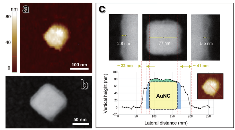
Figure 6. Correlative in situ AFM and SEM data analysis. (a) AFM topography of the same single Au nanocube in the hydrated phase, within deionized water (D.I. H2O), measured using in situ AFM. (b) SEM image of a single Au NC, (c) An example of correlative analysis: SEM image with contrast, revealing the core nanocube and the surfactant layer (including a thin metallic layer) were aligned with the height profile of the same single Au NC extracted from the AFM topography.
For example, Figure 6 illustrates a correlative analysis of a single Au NC, showing its topography measured by in situ AFM (Figure 6a) alongside the corresponding SEM image (Figure 6b). These datasets can be aligned correlatively, as shown in Figure 6c. Aline profile at the center of the Au NC was extracted from the AFM image (black solid line with dots in the bottom panel of Figure 6c). The profile also includes a schematic representation of the Au NC (black dashed line) overlaid on the topography, allowing estimation of the thickness of surface-adsorbed CTAB.
The edge length of the Au NC was 77.0 nm in the SEM image (yellow line in the upper center panel of Figure 6c). The height of the CTAB-adsorbed Au NC (red line in the inset of the lower right AFM image) was approximately 80.0 nm, about 2–3 nm greater than the Au NC edge length (representing the height of the Au NC excluding the CTAB layer). This difference is likely attributable to the presence of surface-adsorbed CTAB, which was sensitively detected by in situ AFM.
Notably, the lateral CTAB thickness exhibited greater variability than the vertical measurements. Under dehydrated conditions (SEM measurement), the CTAB thickness ranged from approximately 2.8 to 5.5 nm (Figure 6c, upper panel). After accounting for a 2 nm metallic coating, the CTAB thickness was 0.8–3.5 nm, consistent with the 2–3 nm vertical height measurements obtained under hydrated conditions.
Under hydrated conditions, the sidewall thickness was estimated by subtracting the SEM-determined width of the Au NC from the full width at half maximum (FWHM) of the AFM topography profile. The CTAB thickness ranged from 22 to 41 nm, significantly higher than in the dehydrated state (Figure 6c, bottom panel, red dashed lines). These results suggest pronounced expansion and redistribution of CTAB in aqueous environments and underscore the importance of evaluating ligand structure under native conditions by in situ AFM.
3D Visualization of CTAB Adsorption Distribution on Single Nanocubesin Hydrated States
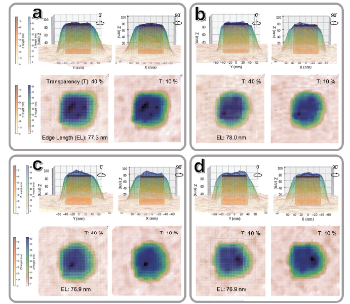
Figure 7. 3D visualization of correlative in situ AFM and SEM measurements of single nanocubes (a-d). Images show four distinct nanocrystals exhibiting heterogeneous ligand adsorption on their top surfaces. Edge lengths were determined from SEM measurements (see Figure 6). Top two rows: side views of image overlay. Bottom row: top views.
Three-dimensional (3D) visualization provides an effective means to illustrate the heterogeneous adsorption of CTAB across the entire surface of the Au NCs, excluding the bottom surface in contact with the substrate. To accurately represent the spatial relationship between the Au NC and the surrounding CTAB layer, a schematic model of the Au NC (yellow) was carefully positioned within the AFM topography-derived surface profile (Figure 7). This placement reflects the likely physical location of the nanocrystal as realistically as possible. The XY position of the Au NC model was carefully adjusted to ensure that all edges of the nanocube were fully enclosed within the topographic contours captured by AFM, allowing for clearer interpretation of CTAB distribution on each facet. As shown in Figure 7a, the first Au NC exhibits this distribution, while three other individual single Au NCs (Figure 7b-d) show CTAB thicknesses of the top surface ranging from approximately 1 ~ 5 nm from AFM, as measured by AFM. These results clearly highlight the heterogeneity of CTAB coverage across different particles and emphasize that CTAB distribution is not uniform across the nanocrystal surfaces.
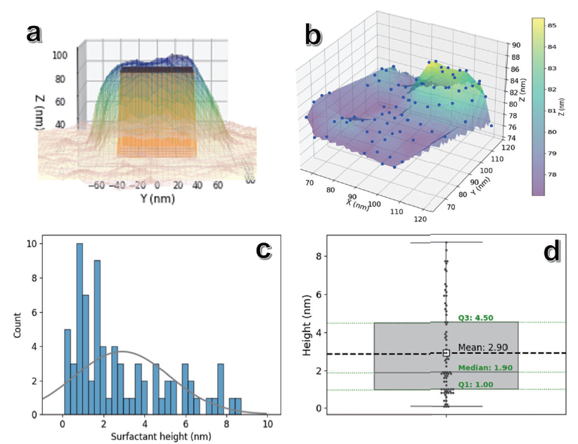
Figure 8. Heterogeneous CTAB molecule adsorption analysis: (a) 3D visualization of correlative in situ AFM and SEM measurements of individual Au NCs. (b) Data points from the top surface of (a) exceeding the nanocube's height (> 76.9 nm), representing CTAB adsorption distribution. (c) Histogram of the data points in (b) with a superimposed normal distribution curve for comparison. (d) Corresponding box plot displaying statistical values of the CTAB adsorption height distribution.
Understanding surfactant adsorption at the molecular level remains a major challenge in modern science, yet it is crucial for advancing nanoparticle and nanocrystal-based applications. In particular, the properties of gold nanoparticles are strongly influenced by the complex interactions among their surface ligands, the surrounding solvent, and the nanoparticle core itself.14-16 The in situ surface profile of CTAB adsorbed on the Au NC, correlated with the carefully aligned 3D dimensions, provides a valuable method to estimate the surfactant distribution on its top surface (Figure 8a). Data points were collected from the corresponding area of the top square surface of a single Au NC. A total of 76 height measurements were obtained (Figure 8b), and the Au NC height of 76.9 nm was subtracted from each data point’s height to isolate the surfactant layer thickness. Using the data set, a statistical analysis was conducted. And the results of this analysis are presented in Figures 8c and 8d. The mean thickness of the CTAB adsorption layer was measured to be 2.9 ± 2.4 nm, which is consistent with the approximate length of a single CTAB molecule (~2.2 nm) as determined using Avogadro software with MMFF94 force fields (Figure 5a). The observed CTAB layer thicknesses range from 1 nm to 10 nm, indicating a highly heterogeneous distribution of CTAB molecules on the Au {100} surface. This indicates the presence of both single molecular layers and multilayer structures, with up to five layers of CTAB adsorbed on the surface.
Conclusions
In conclusion, the experimental example presented in this application note demonstrates that combining in situ AFM and SEM provides researchers with a practical and powerful approach for studying adsorbed surfactant layers and their sensitive molecular interactions with nanocrystal (or nanoparticle) surfaces. In situ AFM, when equipped with appropriate environmental controls and accessories as introduced here, enables the detection of nanometer-scale variations in the adsorption of CTAB molecules on metal crystal interfaces with sub-nanometer resolution in vertical direction (Z axis). This capability is critical for accurately determining the thickness of CTAB layers and assessing their heterogeneity.
By leveraging the topographical data from AFM, together with the precise measurements from SEM, which offer clear contrast between metal and organic materials at identical local positions, this method allows for detailed characterization of surfactant layers only a few nanometers thick on nanocrystal surfaces. To facilitate seamless data acquisition, the sample position linkage system between the Park AFM and JEOL SEM played a crucial role, enabling researchers to capture corresponding data from the exact same location with high accuracy.
The highly colocalized datasets obtained from both techniques make it possible to construct 3D visualizations of heterogeneous surfactant adsorption states. This integrated approach leads to a more comprehensive understanding of nanoscale structures and their properties. Moreover, this methodology is broadly applicable, extending beyond nanoparticles to any microscopic surface that interacts with surfactant molecules.
References
1. Turkevich, John, Peter C. Stevenson, and J. Hillier. The formation of colloidal gold, J. Phys. Chem., 1953, 7.7, 670-673.
2. Elghanian, Robert, et al., Selective colorimetric detection of polynucleotides based on the distance-dependent optical properties of gold nanoparticles. Science, 1997, 277.5329, 1078-1081.
3. Jana, Nikhil R., Latha Gearheart, and Catherine J. Murphy. Seed‐mediated growth approach for shape‐controlled synthesis of spheroidal and rod‐like gold nanoparticles using a surfactant template. Advanced materials, 2001, 13.18, 1389-1393.
4. Ye, Xingchen, et al. Seeded growth of monodisperse gold nanorods using bromide-free surfactant mixtures. Nano letters, 2013, 13.5, 2163-2171.
5. Hu, J. H., et al. Tuning the catalytic activity of colloidal noble metal nanocrystals by using differently charged surfactants. Nanoscale, 2018, 10.12, 5607-5616.
6. Nikoobakht, Babak, and Mostafa A. El-Sayed. Evidence for bilayer assembly of cationic surfactants on the surface of gold nanorods. Langmuir, 2001, 17.20, 6368-6374.
7. Kim, J.; Choi, M.-H.; Jung, G.-E.; Ferhan, A. R.; Cho, N.-J.; Cho, S.-J. Dimensional Comparison Between Amplitude-modulation Atomic Force Microscopy and Scanning Ion Conductance Micros copy of Biological Samples. Jpn. J. Appl. Phys. 2016, 55, No. 08NB18.
8. Choi, M.-H.; Baker, L. A. Biphasic-Scanning Ion Conductance Microscopy. Anal. Chem. 2018, 90, 11797−11801
9. Usukura, J.; Yoshimura, A.; Minakata, S.; Youn, D.; Ahn, J.; Cho, S.-J. Use of the Unroofing Technique for Atomic Force Microscopic Imaging of the Intra-cellular Cytoskeleton under Aqueous Conditions. J. Electron Microsc. 2012, 61, 321−326.
10. Roh, H. S.; Lee, C. M.; Hwang, Y. H.; Kook, M. S.; Yang, S. W.; Lee, D.; Kim, B. H. Addition of MgO Nanoparticles and Plasma Surface Treatment of Three-dimensional Printed Polycaprolactone/ Hydroxyapatite Scaffolds for Improving Bone Regeneration. Mater. Sci. Eng. C 2017, 74, 525−535.
11. Purcar, V.; Raditoiu, V.; Dumitru, A.; Nicolae, C.-A.; Frone, A. N.; Anastasescu, M.; Raditoiu, A.; Raduly, M. F.; Gabor, R. A.; Caprarescu, S. Antireflective Coating Based on TiO2 Nanoparticles Modified with Coupling Agents via Acid-Catalyzed Sol-Gel Method. Appl. Surf. Sci. 2019, 487, 819−824.
12. Necas, D.; Klapetek, P. Gwyddion: an Open-source Software for SPM Data Analysis. Cent. Eur. J. Phys. 2012, 10, 181−188.
13. Schneider, C. A.; Rasband, W. S.; Eliceiri, K. W. NIH Image to ImageJ: 25 Years of Image Analysis. Nat. Methods 2012, 9, 671−675.
14. Pedrazo-Tardajos, Adrián, et al., Direct visualization of ligands on gold nanoparticles in a liquid environment. Nat. Chem., 2024, 16.8, 1278-1285.
15. Li W, et al., Locating the atoms at the hard-soft interface of gold nanoparticles. Nat. Commun. 2026, Jan 12.
16. Sheng H, Dong A. Surface Ligands in Nanocrystal Electrocatalysis: A Double‐Edged Sword. Adv. Mater. 2025 Dec 12:e07862
Related Contents
Solving Thin-Film Uniformity Challenges on Curved Surfaces with Imaging Spectroscopic Ellipsometry

AFM Augmented Sample Fabrication for Next-Generation Layered Materials Devices