


Optical Property - Photoconductivity
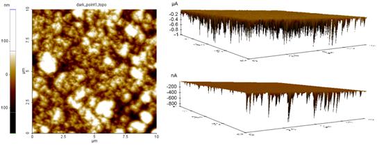
Topography (left image) and photocurrent (right images) with laser source on (top right image) and laser source off (bottom right image) show the effect of light in current generation; note the increased amount of photo-induced current in the upper image.
Park AFM Productivity in Action
Jeongjin Lee, Inhee Choi, Surin Hong, SuSeung Lee, Young In Yang, Younghun Kim, Jongheop Yi; Construction of pcAFM module to measure photoconductance with a nanoscale spatial resolution; Ultramicroscopy 108 (2008) 1090– 1093
Equipment: Park Systems XE-150
Abstract: A photoconductive atomic force microscopy (pcAFM) module was designed and the performance was tested. This module consisted of three units: the conductive mirror-plate, the steering mirror and the laser source. The module with a laser irradiation unit was equipped to a conventional conducting probe atomic force microscopy (C-AFM) instrument to measure photoconductance in a nanoscale resolution.
As a proof-of-concept experiment, the photo-conductance of aggregated fullerene on indium tin oxide (ITO) substrate was measured with this module. The electrical signals (currents) of aggregated fullerene under the conditions of laser on/off at about -10V sample bias voltage were -100 to -160 nA and 0 to -20 nA, respectively. Results indicated that the pcAFM with this module allowed one to observe photoinduced changes of electrical properties in nanodevices with nanoscale spatial resolution.
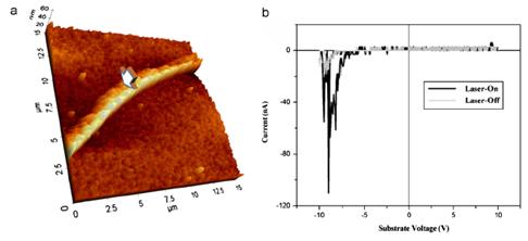
Fig 3. (a)3-D topography of the contact point for the I/V curve measurement and (b) the measured I/V curve. The resistance was decreased by a factor of 5~100. The arrow in (a) indicateds the point at the slope of the sub-circle line, ca, 10 nm height from the boom. At this point, the electrical signals (currents) of aggregated fullerene under the conditions of laser on/off at about -10V sample bias voltage were -100 to -160nA and 0 to -20nA, respectively.
Sample:
- Solar Cell
Image Conditions:
- Contact Mode AFM
- Tr-PCM
- Force ( ?? nN)
- Scan Speed (?? Hz)
System Requirement:
- Closed-loop AFM System
- Conductive AFM
The Benefits
Park AFM series offers many modes that are well suited for phtoonic devices and materials. In particular, Time-resolved Photocurrent Mapping (Tr-PCM) offers the ability to obtain the conductivity data with the AFM laser turned off (at alternative scan lines) so time resolved photo-induced current can be measured:
a) with topography
b) with nanoscale spatial resolution
c) without interference from the AFM laser source.


