


-
MfmAmplitude SicMosfet NCM\ Korea CopperFoil Defect conductive STO 2-vinylpyridine PS_LDPE Hexacontane alkanes Nanopattern Polystyrene Fluoride EFMAmplitude Pores Iron optoelectronics multi_layer dichalcogenide VerticalPFM DeflectionOptics Singapore TemperatureControllerStage NtuEee MfmPhase Layer MetalCompound PhaseChange NanoLithography AmplitudeModulation OxideLayer temperature_control Zhi
Report image
If you found this image unacceptable, please let us know. We will review your report and take action if we determine this image is really unacceptable.
AlN/GaN/AlN Hetero Structure
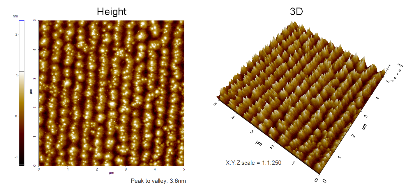
AlN/GaN/AlN hetero structure grown on SiC substrate by Molecular Beam Epitaxy (MBE) system.
Scanning Conditions
- System: NX20
- Scan Mode: Non-contact
- Cantilever: AC160TS (k=26N/m, f=300kHz)
- Scan Size: 5μm×5μm
- Scan Rate: 0.5Hz
- Pixel Size: 512 × 512
- Scan Mode: Non-contact
- Cantilever: AC160TS (k=26N/m, f=300kHz)
- Scan Size: 5μm×5μm
- Scan Rate: 0.5Hz
- Pixel Size: 512 × 512