


Advanced AFM Techniques for Studying Perovskite Materials
Introduction
Perovskites are a class of materials that have emerged as promising candidates for use in photovoltaic cells, which are devices that convert light energy into electricity. Perovskite materials have shown high efficiency in converting sunlight into electrical energy at low cost, making them a potential alternative to conventional silicon-based solar cells. Perovskite solar cells typically consist of a thin layer of perovskite material sandwiched between two electrodes. When light hits the perovskite layer, it creates electron-hole pairs that can be separated and collected by the electrodes to generate an electric current [1]. One of the key advantages of perovskite solar cells is their high efficiency with an increase of reported record efficiency to 26% in just one decade [2]. They are also relatively inexpensive to manufacture, which could make them a promising option for large-scale deployment.
In this application note, we introduce some examples of Atomic Force Microscopy (AFM) modes including Kelvin Probe Force Microscopy (KPFM), Conductive AFM (C-AFM), and Photo Current Mapping (PCM) that can be used to study perovskite material from various perspectives and their potential applications. All experiments were performed in a glove box environment to ensure the most accurate and reliable results were obtained. Because halide-based perovskites are sensitive to temperature and humidity [3], the measurement environment, e.g. oxygen and humidity levels, should be carefully controlled and kept at a minimum to ensure accurate and reproducible measurements. Park Systems provides a precise environmental control system (NX GloveBox with gas purification system) to ensure low water and oxygen concentrations (<35 ppm) by gas purification (Figure 1).
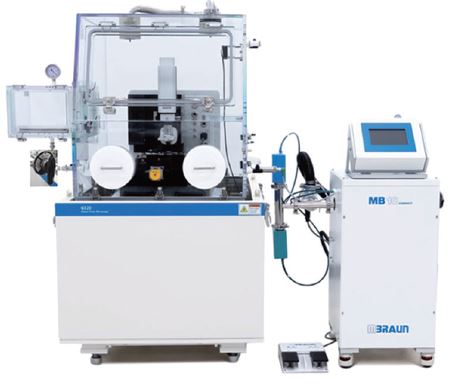
Figure 1. Park Systems NX GloveBox with gas purification system setup and its specifications
| Oxygen and Moisture Level | < 35 ppm (with NX Glove box) |
|---|---|
| Measuring Sensor Range |
Oxygen: 0 - 1000 ppm Moisture: 0 - 500 ppm |
| Automatic Pressure Control Range |
-15 to +15 mbar |
| Working Gas | Nitrogen (N2), Argon (AR) or Helium (He) |
| Box Purging System |
Automatic Control |
| Filter | 1-filter column gas purifier |
KPFM and C-AFM application
KPFM and C-AFM are two techniques that can be used to study different aspects of materials. KPFM is a non-contact surface imaging technique that measures the surface potential of materials with high spatial resolution. In the context of perovskites, KPFM can be used to study the local variation in surface potential and work function of the perovskite layer, which is related to the distribution of charges in the material. KPFM can also be used to measure the built-in potential of the device, which provides information about the energy level alignment between the different layers in the solar cells [4], [5]. Figure 2 shows representative results of sideband KPFM measurements on a perovskite thin film. The sideband KPFM has an advantage in terms of the spatial resolution of the surface potential measurement relative to Amplitude Modulation (AM)-KPFM. It is mainly affected by the AFM tip apex, and it detects the electrostatic force gradient by frequency changes and results in better resolution. The results provide information about the local surface potential of the sample, indicating the presence of different regions with different electronic properties, which can be related to the charge carrier concentration and the presence of defects. These variations could be attributed to variations in the composition, morphology, or defects of the perovskite material.
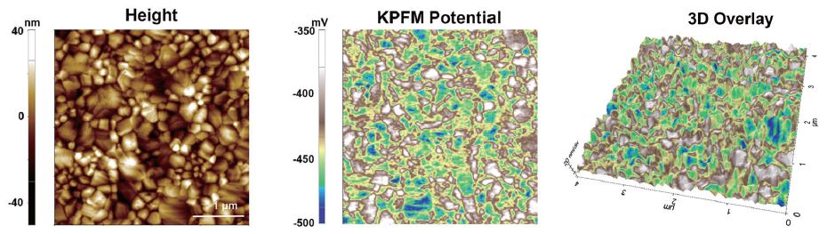
Figure 2. KPFM results (Height, KPFM potential and 3D Overlay (Overlaying the KPFM potential information in the height image) images)on perovskite thin film. Scan size: 4 μm × 4 μm, pixel: 512 × 256, performed by Park NX10.
C-AFM is a contact mode imaging technique that measures the electrical conductivity of materials at the nanoscale. Accordingly, C-AFM can be utilized to study the local conductivity of the perovskite layer, which provides information about the charge transport properties of the material. By mapping the local conductivity of the perovskite layer, C-AFM can help researchers understand the mechanisms that govern charge transport in the material and optimize the performance of perovskite solar cells [6], [7]. In figure 3, the C-AFM measurement was performed by scanning a conductive AFM tip over the surface of the perovskite thin film while applying 0.5 V to the bottom layer. The surface current image revealed that the perovskite film under red light excitation ( Wavelength of 635 nm ) had some localized regions exhibiting slightly higher or lower conductivity, suggesting that there may be regions of higher carrier concentration within the perovskite film.
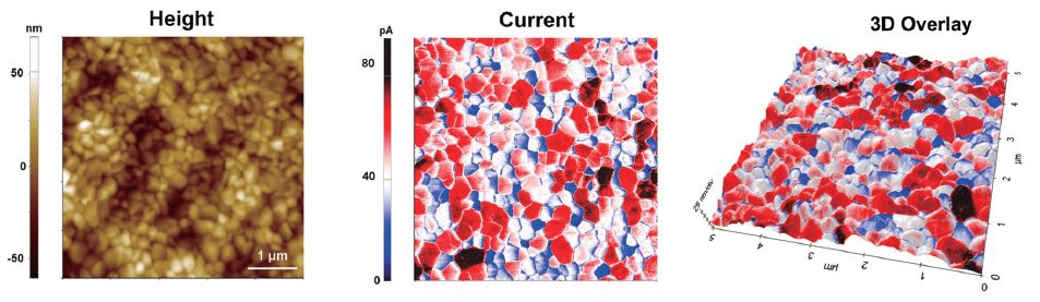
Figure 3. C-AFM results (Height and current images) on perovskite thin film. Scan size: 5 μm×5 μm, pixel size: 512×512,performed by Park NX10. Image courtesy: Kanjanaboos Lab, Mahidol University, Thailand
Observing the photoelectric effect
The photovoltaic effect describes the absorption of light within a semiconductor which promotes an electron from the valence band into the conduction band. In the case of perovskite solar cells, this means that such photo-excited electrons and the remaining positively charged “hole” in the valence band populate a higher energy level within the semiconductor with increased mobility. Accordingly, these charge carriers can migrate through the semiconductor until they reach either the boundary of the perovskite layer or recombine. If the perovskite is sandwiched between two charge-selective layers, where one only allows electrons to pass and the other only allows holes to pass, then the respective cell has rectifying properties and the charge carriers can be collected on either side of this layered structure to harness electric energy [8]. Experimentally, the photovoltaic effect can be studied on a single perovskite layer by illuminating the semiconductor and measuring the local conductance. Since the concentration of free charge carriers increases upon illumination, the measured conductance also increases.
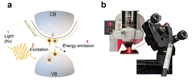
Figure 4. Schematic of photovoltaic effect, 1. Light source exposure, 2. Excitation of electron,3. Electron-hole pair combination, 4. Energy emission of electron (a), Park Systems PCM module,applicable light source: red (Wavelength of 635 nm), blue (405 nm), IR (785 nm) (b).
Park Systems provides an optimal setup for investigating the photovoltaic effect using external laser and sample bias (Figure 4b). Applicable types of light sources are red (Wavelength of 635 nm), blue (405 nm), infrared (IR, 785 nm) of external lasers, and internal LED (White source, 400 ~ 750 nm) and SLD (830 nm). On/off control for external laser and SLD, 0~100 % (Adjustable unit 0.1%) intensity control for LED is possible. The light source and sample bias are controlled as synced parameter by SmartScanTM (AFM operation software, Park Systems). General PCM measurement process is mainly three steps, 1. Reset bias (A+B in figure 5), 2. Applied bias with light driving (C in figure 5), 3. Resting (F-A+B+C in figure 5). The reset bias serves to neutralize any remaining charges in the measurement area. Sufficient time is required for the current to stabilize. Applied bias and the light source of time duration can be specified by the user so that spectroscopy of photovoltaic reaction is measured as current variation through time (Figure 5).
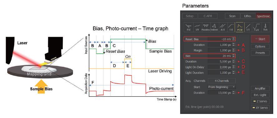
Figure 5. Park Systems’ PCM operation process and related parameters
Figure 6 shows measurements of the electrical properties of a formamidinium lead iodide (FAPbI3) film using KPFM and C-AFM. To investigate the photovoltaic effect, the LED light intensity was adjusted, and the electrical properties were measured (KPFM; Potential and Work function, C-AFM; Current) with respect to the light intensity. FAPbI3 is a type of hybrid organic-inorganic perovskite material that has been widely investigated for use in photovoltaic solar cells. It has properties that allow for efficient light absorption and charge transport, making it a promising candidate for next-generation solar cell technology. As mentioned above, when perovskite materials absorb light, they generate free charge carriers (electrons and holes), which can then be separated and collected as electrical current. The electrical properties of perovskite materials are strongly influenced by the intensity of light absorption. As the intensity of LED increases, more free charge carriers are generated, leading to an increase in the electrical current that can be extracted from the material. In KPFM images, changes in potential and work function according to the intensity of light can be confirmed. As the intensity of light increases, the contrast does not appear clearly due to saturation. The C-AFM image also shows a similar trend to that of KPFM, but a clearer contrast is identified in each step. Typically, perovskite solar cells exhibit a nonlinear response to changes in light intensity [9]. At low light intensities, the current generated by the cells is proportional to the light intensity. However, at higher light intensities, the current saturates and becomes independent of further increases in light intensity. This nonlinear response is attributed to a combination of factors, including the limited diffusion length of charge carriers, which can lead to recombination and loss of charge carriers at high light intensities, and the finite lifetime of the charge carriers, which limits the amount of charge that can be collected before recombination occurs.
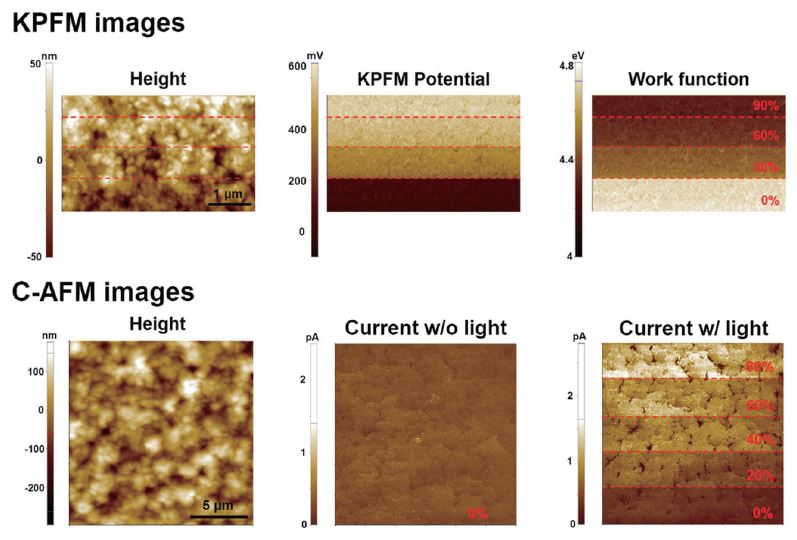
Figure 6. Changes in electrical properties according to light intensity of perovskite thin film, measured by KPFM and C-AFM. Red fonts indicate induced light intensity. Scan size: 5 μm×4 μm,pixel size: 512×256 for KPFM, scan size: 15 μm×15 μm, pixel size: 512×256 for C-AFM, performed by Park NX10.
Conclusion
Perovskite solar cells hold great promise as a low-cost and highly efficient alternative to traditional silicon solar cells. To fully realize this potential, it is essential to have access to the appropriate methods, equipment, and environment to study and improve the performance of these materials. AFMs including KPFM and C-AFM are powerful tools for studying different aspects of the perovskite material. Moreover, the C-AFM setup can be equipped with an external laser module to investigate the photoconductive properties time-resolved using our PCM which allows us to study the photo-decay and thus shines light on recombination and trap density within a photo absorber. By correlating high-resolution information about the surface potential and conductivity of the perovskite layer with topographical information, these techniques can help researchers optimize the performance of perovskite solar cells and develop more efficient and durable solar cell technologies. Lastly, Park Systems provides an optimal environment to research perovskite/perovskite solar cells. by giving control over the measurement environment such as temperature and humidity which drastically facilitates future research on this material.
References
1. Jung, H. S., & Park, N. G. (2015). Perovskite solar cells: from materials to devices. small, 11(1), 10-25.
2. https://www.nrel.gov/pv/interactive-cell-efficiency.html
3. Yun, J. S., Kim, J., Young, T., Patterson, R. J., Kim, D., Seidel, J., ... & Ho‐Baillie, A. (2018).
Humidity‐induced degradation via grain boundaries of HC (NH2) 2PbI3 planar perovskite solar cells. Advanced Functional Materials, 28(11), 1705363.
4. Kang, Z., Si, H., Shi, M., Xu, C., Fan, W., Ma, S., ... & Zhang, Y. (2019). Kelvin probe force microscopy for perovskite solar cells. Sci. China Mater, 62(6), 776-789.
5. Bergmann, V. W., Weber, S. A., Javier Ramos, F., Nazeeruddin, M. K., Grätzel, M., Li, D., & Berger, R. (2014). Real-space observation of unbalanced charge distribution inside a perovskite-sensitized solar cell. Nature communications, 5(1), 5001.
6. Si, H., Zhang, S., Ma, S., Xiong, Z., Kausar, A., Liao, Q., ... & Zhang, Y. (2020). Emerging conductive atomic force microscopy for metal halide perovskite materials and solar cells. Advanced Energy Materials, 10(10), 1903922.
7. Leblebici, S., Leppert, L., Li, Y. et al. (2016). Facet-dependent photovoltaic efficiency variations in single grains of hybrid halide perovskite. Nat Energy 1, 16093.
8. Kayesh, M. E., Chowdhury, T. H., Matsuishi, K., Kaneko, R., Kazaoui, S., Lee, J. J., ... & Islam, A. (2018). Enhanced photovoltaic performance of FASnI3-based perovskite solar cells with hydrazinium chloride coadditive. ACS Energy Letters, 3(7), 1584-1589.
9. Glowienka, D., & Galagan, Y. (2022). Light intensity analysis of photovoltaic parameters for perovskite solar cells. Advanced Materials, 34(2), 2105920.