


AFM experts provide you ONLINE courses, easy and comfortable to join from home! FREE access for you to all content: Webinars, Live Demos, Educational Videos, Software Operation, NanoScientific Talk! Microscopy research has never been so easy before!
Upcoming Webinar
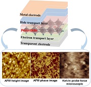
Application of Atomic Force Microscopy in perovskite solar cells (Chinese/中文)
Wednesday, April 29, 2020 / 10:00am CST
As one of the most powerful scanning probe microscopy (SPM) techniques, atomic force microscopy (AFM) can not only detect...
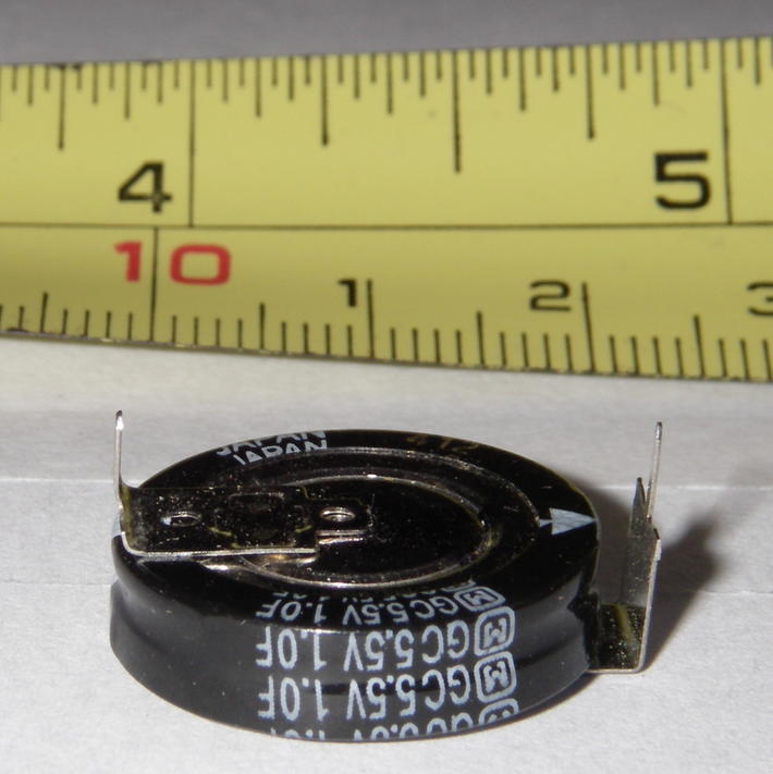
Investigation of Lithium Ion Battery Electrodes Using Pinpoint SSRM in Vacuum
Wednesday, April 29, 2020 / 9:00 am PDT
The applications staff of Park Systems is proud to present an introduction to PinPoint scanning spreading resistance microscopy (SSRM).
Advanced Piezoresponse Force Microscopy
Wednesday, April 29, 2020 / 11:00 am CST
The application the ferroelectric materials in communication and information technology or data storage continuously increases.
Live Demo
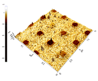
From automatization in research to quality control for industrial applications
Wednesday, April 22, 2020/ 9:30 am GMT
Learn how automation features in AFM can easily be implemented into your workflow to boost the productivity in your lab.
SmartScan Advanced KPFM Imaging
Friday, April 24, 2020 / 12:00 pm PDT
Measuring the electrostatic interaction between the atomic force microscope (AFM) tip and sample is a common technique used to characterize electrically sensitive samples.
Full-automation AFM in-line capabilities
Wednesday, May 6, 2020 / 3:00 pm GMT
In this LIVE DEMO on the NX-Wafer Automated AFM we will introduce you to the inline metrology capabilities which are needed for full-automatic quality control.
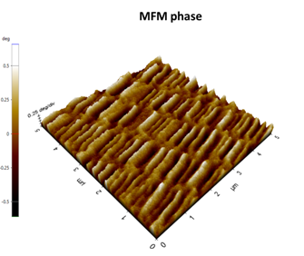
SmartScan MFM Imaging
Friday, May 1, 2020 / 12:00 pm PDT
Magnetic force microscopy (MFM) is a Park Systems advanced AFM mode used for studying surfaces with magnetic properties by detecting the interaction between a magnetized cantilever...
Quick automation set-up for research applications
Wednesday, April 15, 2020/ 9:30 am GMT
In this Live Demo we will walk you through the quick automation set-up for research applications by using SmartScan & StepScan.
SmartScan Topography Imaging
Friday, April 17, 2020/ 12:00 pm PDT
Park Systems Weekly Demo & Chat Sessions is a new series of online, live demonstrations of Park AFM Systems hosted by the Park Systems Technical team. Each week, an engineer from the technical team...
Webinar Recordings

Nanotechnology in Plastics and Packaging
The Park Systems 2019 Materials Matter Material Science Research and AFM Webinar Series continues with Nanotechnology in Plastics and Packaging.

Surface Plasmon Resonance Spectroscopy Tandem with AFM
The Park Systems 2019 Materials Matter Material Science Research and AFM Webinar Series continues with Surface Plasmon Resonance Spectroscopy Tandem with AFM.
Viscoelastic Surfactants and Oilfield Chemicals
The Park Systems 2019 Material Science Research and AFM Webinar Series continues with Viscoelastic Surfactants and Oilfield Chemicals.
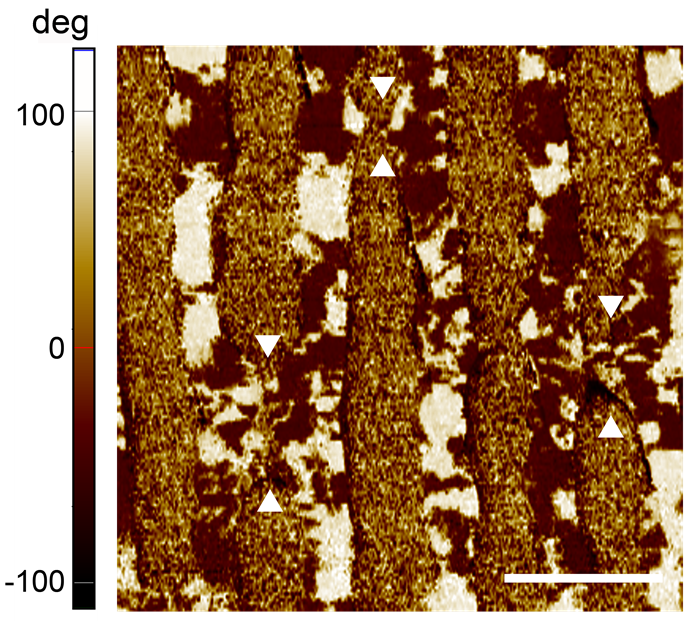
Physical Properties of Emergent 2D materials with AFM
In this webinar, the reporter will share some of the experience of using Park AFM (XE 100 and NX10). Since 2011, the reporter has used Park AFM as the main research tool, and made some interesting researches in the study of 2D material properties, the characterization of optoelectronic devices, and the exploration of novel 2D material electronic devices.
2D Nanomaterials for Smart Coatings and Fluids
2-D nanomaterials are known for its property of being only one or two atoms thick. Due to their high ratio of surface area to volume, they immensely benefit from unique physical, chemical, and biological functionality.
Electrochemical Capacitors: Fundamentals, Materials, and Advanced Characterization
This webinar is the first of a two-part webinar series focused on ECs. The first webinar is focused on the fundamental of charge storage in ECs and recent advances in the development of materials for these devices.
Nanostructured Polymer Brushes With AFM
The Park Systems 2019 Material Science Research and AFM Webinar Series kicks off with Nanostructured Polymer Brushes With AFM, focusing on how Atomic Force Microscopy is a vital tool in characterizing the morphology of grafted polymer brushes.
Educational Webinars “AFM Techniques”
Atomic Force Microscopy PinPoint Nanomechanical Mode for Nanoscale Modulus Mapping – Cantilever Modulus and Applied Force
The applications staff of Park Systems will give this webinar on atomic force microscopy PinPoint Nanomechanical Mode for Nanoscale Modulus Mapping, specifically, we will look at the influence of cantilever stiffness and applied force on the measured modulus.
PinPoint Piezoelectric Force Microscopy
PFM functions by engaging a sample surface with a sharp conductive SPM probe. This probe's tip then has an alternating current (AC) bias applied to it in order to cause a deformation of the sample surface by way of a piezoelectric force.
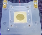
Electrochemical Atomic Force Microscopy (EC-AFM)
In EC-AFM, users typically perform voltamemetry and corrosion experiments using an electrochemistry cell and a choice of potentiostat or galvanostat depending on the electrochemical application of interest.
PinPoint Nanomechanical Imaging Using Probes of Various Cantilever Stiffness
PinPoint Nanomechanical mode obtains the best of resolution and accuracy for nanomechanical characterization. Stiffness, elastic modulus, adhesion force are acquired simultaneously in real-time.
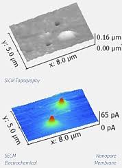
Scanning Ion Conductance Microscopy (SICM) and Scanning Electrochemical Microscopy (SECM)
SICM uses the increase of access resistance in a nanopipette placed in an electrolyte solution and monitors the ionic current flowing in and out of this probe—a flow that is hindered as the tip closes in on a sample surface.