


Park Systems presents Nanoscale Solutions for Design and Manufacturing of Electronic Devices – a digital workshop series


This focused workshop series will provide an opportunity to Design, Process, Metrology, Yield and Failure Analysis Engineers to interface directly with Park Systems’ advanced applications experts and discuss day-to-day nanoscale solutions that address device manufacturing challenges.
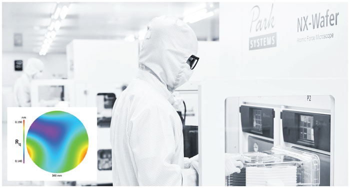
Nanoscale Solutions for Design and Manufacturing of Electronic Devices – a digital workshop series
Register for the first workshop , held on June 25th
WHY PARK SYSTEMS ATOMIC FORCE MICROSCOPES
- • Leader in Automated AFM Equipment
- • Industry's sole non-destructive inspection and metrology technology, bundled in a single instrument
- • Lower in-fab costs compared to individual inspection or metrology tools
- • Fully-automated fleet matching tools enable day-to-day solutions for manufacturing yield challenges
- • The choice of many of the top 20 Semiconductor Manufacturers
WHY PARK SYSTEMS ATOMIC FORCE MICROSCOPES
- • Device Scaling and Novel Structure Designs
- • Process Advancements to Enable High Volume Manufacturing Solutions
- • Inspection and Metrology Methods to Capture Yield Excursion
- • Packaging and Reliability Considerations.