


SmartScan Lithography - May 22, 2020


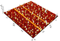
Park AFM’s nanolithography is an advanced AFM technique used to pattern nanoscale shapes onto sample surfaces. In the bias-assisted or anodic oxidation method, a bias voltage is applied to the tip to generate an oxide pattern on a metallic or semiconductor substrate. In this session, we will demonstrate how to create nanometer sized structures and discuss the main parameters to consider during the process using SmartScan™ Nanolithography on the Park NX10 AFM system.