


Laura Piperno
Laura is a PhD candidate at the Engineering Department (Applied Electronics), Roma Tre University. Her current research project is titled “Artificial pinning engineering in high-performance superconducting thin films obtained via chemical solution deposition.”
Since its discovery, superconductivity has presented a huge application potential, primarily for the possibility of carrying current without dissipating energy. The two main classes of materials studied are: the high temperature superconductors (High Temperature Superconductors, HTS), which exhibit a critical transition temperature higher than that of liquid nitrogen, and low critical temperature superconductors, which are instead superconducting at temperatures close to absolute zero. For large-scale applications, naturally the compounds belonging to the first category are preferred, by virtue of the possibility of refrigerating these low-cost systems. The required performance of HTS is still under development, in particular the high density of critical current obtainable at high magnetic fields at temperatures close to 77 K. Also, the great development costs have prevented the technology to spread. The first HTS cables, called "first generation" cables, with unpromising performances, were overcome by second-generation conductors in the form of strips based on YBa2Cu3O7-δ (YBCO) - a ceramic compound belonging to the cuprates family, like many of the HTS. They are obtained from epitaxial films of YBCO grown on metallic tapes- a process still under study for the industrial scale development of superconducting tapes (also called coated conductors).
Please summarize the research you do and explain why it is significant?
I am currently working on artificial pinning engineering for chemically derived YBa2Cu3O7-x (YBCO) films. My research is focused on developing new all-chemical strategies for enhancing the YBCO transport properties that are suitable for a future industrial scale-up. My group and I are currently working on the preparation of oxide nanostructured templates for the deposition of YBCO and the introduction of secondary phases with both in-situ and ex-situ techniques. Great effort is put in the comprehension of the pinning mechanisms in order to be able to tune the properties of the samples according to specific needs.
More in detail, my project requires the preparation of the chemical precursor solutions for the aforementioned systems, the deposition of the solutions and growth of the samples via different thermal treatments. Once the samples have been prepared, routine characterizations are carried out.
How might your research be used?
My contribution to the field is to exploit my knowledge as a material chemist to design pinning strategies that fulfil the requirements, such as atomic substitutions/vacancies, or the synthesis and introduction of pre-formed secondary phases of the right size. This technology is to be transferred to tapes and HTS cables. This topic is a great challenge, but I think that the combination of the chemical and engineering approach to the problem could lead to great advancements in this research field, that is a fundamental part of the road towards clean fusion energy.
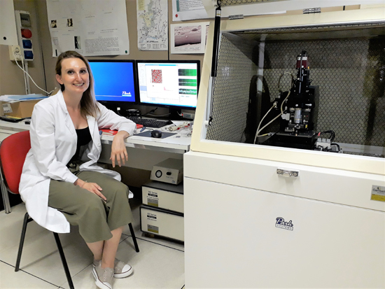
Why is the Park AFM important for your research?
The thorough characterization of the prepared templates is essential in this project. Since the size, density and distribution of the nanostructures on the substrate might have an influence on the properties of the final superconducting film, it is important to keep track of the characteristics of each sample. Once the impact, which they have, is understood, it will be possible to tune these characteristics in the desired direction.
What features of Park AFM are the most beneficial and why?
For my project, I am most interested in the morphology of the samples, so I take and analyze the topography images. The nanostructure I need to characterize are very small (15-30 nm diameter, 5-10 nm height). AFM scans of the surfaces are usually carried out in the true non-contact mode. Once the image is taken, statistical analysis of the nanostructures is carried out. Parameters such as mean height and diameter of the nanoparticles and surface roughness are evaluated.