


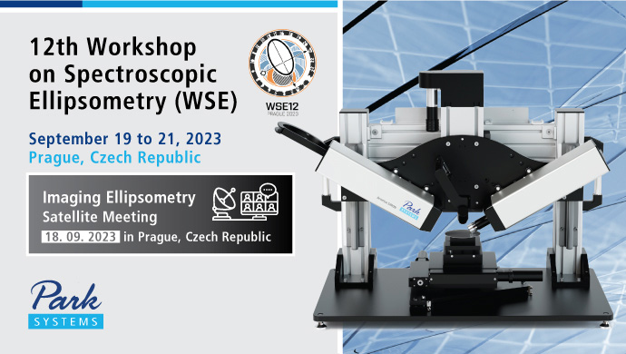
The 12th Workshop on Spectroscopic Ellipsometry (WSE) will take place during the week of September 19 to 21, 2023 in Prague, in the Czech Republic. There will also be a satellite meeting on Imaging Ellipsometry before the main event on the 18th and another satellite meeting on Time-resolved Ellipsometry right afterwards on the 22nd of September. Park Systems is proud and excited to be sponsoring this event, as well as co-organizing the pre-workshop satellite meeting.
The goal of the workshop and satellite meetings is to provide an international platform to discuss developments in Ellipsometry and related methods of metrology from science to industrial applications. It is also particularly aimed at young researchers and scientists to encourage an interdisciplinary exchange of expertise and experience.
- • Event Date Satellite Meeting: 18 September 2023
- • Event Date WSE: 19 – 21 September 2023
- • Venue: The SOLID21 building of the Institute of Physics of the Czech Academy of Science, Prague, Czech Republic
The Accurion imaging ellipsometers (EP4, SIMON) use a combination of ellipsometry and microscopy to enable surface characterization with the highest lateral ellipsometric resolution down to 1 µm. We will be featuring a SIMON at our booth, book a demo slot if you want a live demonstration with your own sample.

____________________________________________________________________________________________________________
Join us for our talks:
- ⏩ TITLE: “Systematic analysis of the Rayleigh–Wood anomalies and the symmetry relations of 2D‐periodic nanostructures by imaging spectroscopic ellipsometry”
- ⏩ PRESENTER: Shun Okano, Application Scientist, Park Systems GmbH (former Accurion GmbH), Göttingen, Germany
- ⏩ DATE: Tuesday 19 September 2023, 16:00 – 16:15
ABSTRACT
Co-Author: Matthias Duwe¹, Murat Sivis²,³, Gen Ueda⁴, Tetsuhiro Owa⁴ and Kenji Ikushima⁴
¹ Park Systems GmbH (former Accurion GmbH), Göttingen, Germany
² Department of Ultrafast Dynamics, Max Planck Institute for Multidisciplinary Sciences, Göttingen, Germany
³ 4th Physical Institute, Georg‐August‐Universität Göttingen, Göttingen, Germany
⁴ Department of Applied Physics, Tokyo University of Agriculture and Technology, Koganei, Tokyo, Japan
Modern microfabrication technology enables the production of submicron- and nanometer-order structures without difficulty, with manifold applications in both scientific research and industrial production. Spectroscopic ellipsometry has been widely used to investigate sub-micron periodic structures. However, conventional ellipsometry requires the structured sample region to be larger than the probing spot size, with spot diameters typically in the range of hundred microns to several millimeters for such applications. Any reduction of nanostructure patch sizes is desirable to reduce fabrication time and cost and to yield a higher throughput per wafer. Spectroscopic imaging ellipsometry offers the major benefit that the structured sample region may be many times smaller the probing spot. In this study, we demonstrate the characterization of multiple 50 µm x 50 µm square patches of periodic gold nanostructure arrays, fabricated by electron beam lithography on a native Si substrate. A total of 25 patches with different structural parameters was measured simultaneously for a 360° azimuthal rotation of the sample, allowing for a systematic analysis of the grating constants and structure sizes. The measured Delta/Psi and Mueller matrix spectra showed the characteristic Rayleigh-Wood anomalies of the periodic structure that correspond to diffraction orders propagating within the sample plane (Rayleigh line). We confirmed that two types of this anomaly fell into the investigated spectral range. The Rayleigh lines of the atmosphere-to-grating interface appeared in the ultraviolet to visible spectral range, whereas the much higher refractive index of the Silicon substrate shifted the respective lines of the grating-to-substrate interface into the near-infrared range. The Mueller matrix spectra in the visible range revealed a minor deviation from the expected 2-fold rotational symmetry. A biaxial layer modelling, assuming a slight c-axis tilt reproduced the effect, which may be interpreted as a minute mirror asymmetry of the produced nanostructures.
[1] Shun. Okano et. al., Appl. Res. e202200088 (2023)
____________________________________________________________________________________________________________
Join us at Poster Session 2 on Wednesday 20 September 2023
from 12:30 - 14:00

- ⏩ TITLE: "Characterization of Single Crystals of Methylamonium-Lead-Bromide-Perovskite by Imaging Spectroscopic Ellipsometry (ISE)"
- ⏩ PRESENTER: Dr. Peter Thiesen, Sales Manager and Application Specialist at Park Systems GmbH, Göttingen, Germany
- ⏩ Poster 17
ABSTRACT
Co-Author: Shun Okano, Matthias Duwe, Stefan Schneider
After the WSE2019, there have been a number of future-oriented innovations in the field of imaging ellipsometry. Perhaps the most important innovation is a completely new measurement mode that dramatically reduces measurement times for spectroscopic mapping. We will explain this in more details and also present other very helpful hardware and software innovations.
- ⏩ TITLE: "From Macro to Nano – How Does the Combination of Imaging Spectroscopic Ellipsometry and Scanning Force Microscopic Methods Enable a Deeper Understanding of Complex Surface Systems?"
- ⏩ PRESENTER: Dr. Peter Thiesen, Sales Manager and Application Specialist at Park Systems GmbH, Göttingen, Germany
- ⏩ Poster 18
ABSTRACT
Co-Author: Dr. Alexander Klasen, Dr. Andrea Cerreta, Dr. Jens Böttcher
Imaging spectroscopic ellipsometry (ISE) is based on the interaction of polarized light with the material surface under reflecting conditions. Atomic Force Microscopy (AFM) allows to measure acting forces on a nanometer scale, for example to study mechanical interactions or electrical properties.
Imaging spectroscopic ellipsometry and AFM have a similar sensitivity regarding layer thickness but a completely different lateral resolution. Imaging ellipsometry offers a microscopic view and in combination with x,y scanning and stitching even super images of mm to wafer size with a microscopic resolution. However, the technique is ultimately limited to the Abbe diffraction limit and other optical effects. A lateral resolution in the nm range or even atomic resolution images are, however, the strength of AFM.
The synergetic advantage of combining ellipsometry with AFM can be emphasized using 2D materials as an example. Localizing and identifying a respective piece, flake or crystal is one of the main challenges in characterization of exfoliated 2 D materials.
From the macroscopic point of view, ellipsometric contrast micrographs or microscopic maps of Delta and Psi can be stitched and offer a fast, non-contact, wafer-scale, atomic layer resolved imaging of 2D materials on a variety of substrates. Including maps recorded at different wavelengths, a specific search for microcrystals with a dedicated number of layers or a predefined thickness has been reported.
From the nanoscopic point of view, methods like Kelvin probe force microscopy (KPFM) provide information on structure and electrical properties at the same time and the data analysis can illuminate how the surface potential difference and the work function correlate with the thickness, size and shape.
Combining information from both methods like including the topological information from AFM into the optical modelling of an imaging ellipsometer offers a microscopic view on the optical properties of smallest particles as well as the correlation between optical properties and topology or mechanical and electrical information recorded with scanning probe method.
_____________________________________________________________________________________________________________
About The Workshop of Ellipsometry (WSE)
The Workshop of Ellipsometry (WSE) has taken place since 2000, gathering an increasing number of scientists from all over the world.The aim of this workshop is to provide a platform to present new advances and developments in ellipsometric application, science, and technology and related methods of metrology as well as to encourage interdisciplinary research, and to discuss topics such as metamaterials, rough and structured surfaces, electronic properties, organic and biological materials, photovoltaics, microelectronics, metrology, hardware and software and much more.