


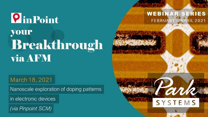
Nanoscale exploration of doping patterns in electronic devices (via PinPoint SCM)
18 March, 2021
- 10:00 am – 11:30 am
(GMT)
London, Dublin - 11:00 am – 12:30 pm
(CET)
Berlin, Paris, Rome - 18:00pm – 19:30 pm
[UTC+9]
Seoul, Tokyo

With the downscaling of electronic devices to the nanoscale, an accurate, high-resolution characterization of structural and electronic properties becomes increasingly important. Atomic Force Microscopy (AFM) offers real space imaging with a nanometer resolution, and not only measures the topographic features, but can simultaneously detect nanomechanical and electrical properties.
Scanning Capacitance Microscopy (SCM) is a versatile tool in the semiconductor industry for failure analysis and measuring doping profiles with the advantage of being a non-destructive method with high spatial resolution. Applications range from characterizing ion implanted semiconductors, electrical properties of Metal-Oxide-Semiconductor (MOS) devices and non-volatile ultra-high density memories.
In this webinar, we will explore the capabilities of SCM for electronic device applications. We will show the additional options that can be added to traditional SCM using our SmartScan(TM) software for improving measurement results and repeatability. In particular, we will show PinPoint(TM) measuring mode in combination with SCM. PinPoint(TM) is the nanomechanical mode from Park Systems which allows to completely remove the lateral impact of AFM measurements from the electrical scan. This heavily increases the repeatability as the tip/sample interaction is much more controlled and not impacted by lateral movement. Furthermore, nanomechanical properties can be recorded at the same time as the SCM signal is measured.
Combining SCM with Park Systems’ PinPoint(TM) mode allows overcoming these issues. PinPoint(TM) avoids the lateral movement of the tip on the sample surface and thus, prevents damage to the tip and sample. Furthermore, the well-defined tip-sample contact reduces topographic crosstalk. We will demonstrate those measurements live on our Park Systems’ NX10 High Resolution AFM on a SRAM sample.
Presented By :
Dr. Andrea Cerreta, Application Scientist Park Systems Europe, Mannheim, Germany
acerreta@parksystems.com
Dr. Andrea Cerreta is an Application Scientists at Park Systems Europe, where he focuses on application development and support for the academic sector. He received his Ph.D. in Physics from the Ecole Polytechnique Fédérale de Lausanne (EPFL), Switzerland. He did his further doctoral work at the Solid State Physics Group of Université de Fribourg, Switzerland, which focused on studying electrical and magnetic properties of organic spin valves and spin polarized currents in superconducting materials, grown by means of Pulsed Laser Deposition, and characterizing the DC and AC transport properties of magnetic and superconducting samples. His expertise also spans the Frequency Modulation Atomic Force Microscopy in UHV for the study of biomolecules.