


-
ConductiveAFM ImideMonomer MagneticPhase Plug SingleLayer TemperatureControllerAFM Fujian CrystalGrowing LateralForce HexagonalBoronNitride Celebration bias_mode Liquid BreastCancerCell BoronNitride AtomicLayer semifluorinated_alkanes WWafer Piezoresponse YszSubstrate SiliconCrystal BFO nanobar ThermalConductivity GlassTemperature PolyimideFilm Singapore Edwin Current food PhaseTransition AnodizedAluminumOxide aluminum_nitride LeakageCurrent Tungsten
Report image
If you found this image unacceptable, please let us know. We will review your report and take action if we determine this image is really unacceptable.
Photoresist pattern (post-development process)
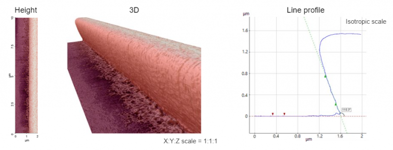
Scanning Conditions
- System : NX-3DM
- Scan Mode: Non-contact
- Scan Rate : 0.1 Hz
- Scan Size : 2μm×10μm
- Pixel Size : 512×2048
- Cantilever : EBD-R2-NCLR (k=45N/m, f=190kHz)