


-
SingleCrystal epitaxy Gallium high_resolution Chrome lithography ItoGlass SiliconeOxide SmallScan TungstenThinFilmDeposition AtomicLayer Lift CNT Chromium BTO ContactModeDot PolyvinylideneFluoride PvdfBead Ptfe plastic Pipette Croatia Oxide AEAPDES cannabis BiFeO3 Annealing conductive Protein Tungsten_disulfide 2dMaterials mono_layer BiasMode Polyvinylidene Grain
Report image
If you found this image unacceptable, please let us know. We will review your report and take action if we determine this image is really unacceptable.
Trench Etch Profile on Si Wafer
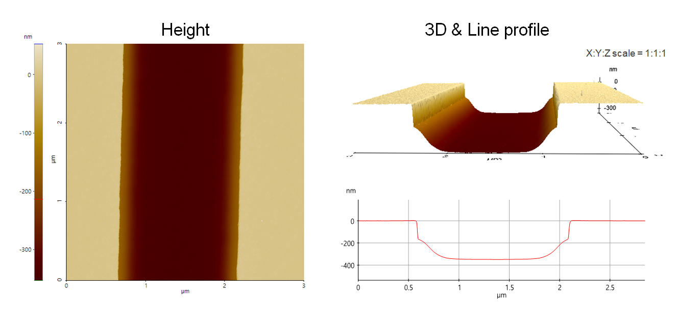
Top dielectric trench etch profile on Si wafer having tapered slope at the trench sidewall.
Scanning Conditions
- System: NX20
- Scan Mode: Non-contact
- Cantilever: AC160TS (k=26N/m, f=300kHz)
- Scan Size: 3μm×3μm
- Scan Rate: 0.21Hz
- Pixel: 1024 × 256
- Scan Mode: Non-contact
- Cantilever: AC160TS (k=26N/m, f=300kHz)
- Scan Size: 3μm×3μm
- Scan Rate: 0.21Hz
- Pixel: 1024 × 256