


-
TemperatureControllerStage CeNSE_IISc TemperatureControlledAFM HighAspect CarbonNanotube TungstenThinFilmDeposition Solar Wonseok PolyimideFilm Microchannel Array OpticalModulator BCZT CuFoil Phenanthrene Co/Cr/Pt nanobar Fendb Singapore Typhimurium Oxide frequency_modulation epitaxy flakes GaAs StainlessSteel Floppy LeakageCurrent DIWafer temperature controller AFM 2d_materials Collagen Chungnam_National_University vertical_PFM HACrystal
Report image
If you found this image unacceptable, please let us know. We will review your report and take action if we determine this image is really unacceptable.
Multi-layer necking device defect
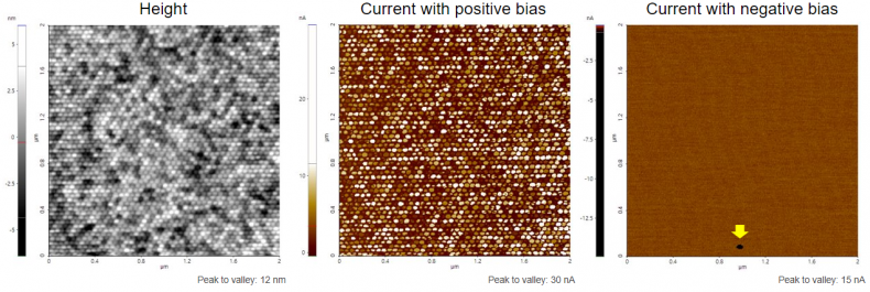
Scanning Conditions
- System : NX-Wafer
- Scan Mode: C-AFM
- Scan Rate : 2Hz
- Scan Size : 2μm×2μm
- Pixel Size : 512×256
- Cantilever : AD-2.8-AS (k=2.8N/m, f=75kHz)