


-
H-BN NanoLithography Vanadate nanobar alkanes PDMS DIWafer rubber AM_SKPM FrictionalForceMicroscopy Indent PVAC chemical_compound Sperm SAM neodymium_magnets TungstenDeposition ferromagnetic Layer Workfunction GlassTemperature Perovskite Metal-organicComplex HydroGel temperature_control Scanning_Thermal_Microscopy Ecoli Aggregated_molecules CrystalGrowing Annealing Edwin Celebration PolycrystallineFerroelectricBCZT Fluoride BaTiO3
Report image
If you found this image unacceptable, please let us know. We will review your report and take action if we determine this image is really unacceptable.
GaN epi wafer
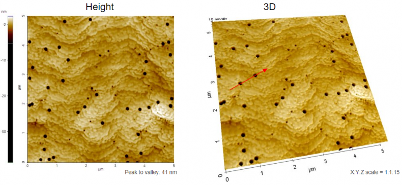
Scanning Conditions
- System : NX-Wafer
- Scan Mode: Non-contact
- Scan Rate : 0.7 Hz
- Scan Size : 5μm×5μm
- Pixel Size : 512×512
- Cantilever : PPP-NCHR (k=42N/m, f=330kHz)