


-
Metal-organicComplex mechanical property ForceVolumeMapping CVD Electronics Temperature AM_KPFM Steps AlkaneFilm Multiferroic_materials fluoroaalkane VortexCore Gallium_Arsenide Polarization ContactModeDots Typhimurium Battery ForceMapping TemperatureControlledAFM DomainSwitching block_copolymer ContactModeDot high_resolution thermal_conductivity domain_switching Foil ReflexLens Gong Bismuth Crystal Copper Reduction Non-ContactMode HiVacuum optoelectronics
Report image
If you found this image unacceptable, please let us know. We will review your report and take action if we determine this image is really unacceptable.
MoS2 Layers on SiO2
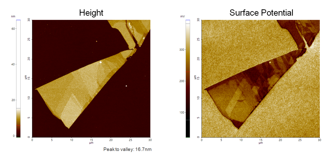
A few layers of MoS2 on SiO2
Scanning Conditions
- System: NX10
- Scan Mode: AM-KPFM
- Cantilever: NSC36Cr-Au B (k=2N/m, f=130kHz)
- Scan Size: 30μm×30μm
- Scan Rate: 0.3Hz
- Pixel Size: 512 × 256
- Scan Mode: AM-KPFM
- Cantilever: NSC36Cr-Au B (k=2N/m, f=130kHz)
- Scan Size: 30μm×30μm
- Scan Rate: 0.3Hz
- Pixel Size: 512 × 256