


Characterizing the displacement and voltage induced on a piezo/photodiode device by pulsed laser excitation via time resolved Kelvin Probe Force Microscopy
Andrea Cerreta1, Zeinab Eftekhari2, Rebecca Saive2, Alexander Klasen1
1Park Systems Europe, Germany
2Inorganic Materials Science, MESA+, University of Twente, Enschede, 7522NB, the Netherlands
Introduction
Energy from different natural sources (light, wind, thermal, etc.) can be converted into measurable electrical quantities via a series of physical phenomena, some of which are at the basis of modern-day technologies. Among devices where energy conversion plays a central role, this application note focuses on piezo actuators and photodiodes.
The piezoelectric effect describes the insurgence of a potential difference at two opposite sides of certain materials once that a mechanical strain is applied to them. This is intimately related to the fact that the deformation of the crystalline structure results into the creation of dipoles at the unit cell level. Also, the same materials exhibit a similar effect in the opposite way, i.e. a mechanical deformation is observed when a voltage is applied to a piezoelectric sample. Piezoelectricity has a wide application in the fabrication of scanners and positioners.
Photodiodes are semiconductor-based devices which have their main practical use as light detectors. Their working principle lies on the fact that once the photodiode surface is illuminated by light, a voltage proportional to the intensity of the impinging beam is generated. In the case of a time-modulated light signal such as a sinusoidal or pulsed wave, a photodiode allows converting its amplitude, frequency and phase into electrical signals that can be analogically measured. Photodiodes can then be used to wirelessly transfer both energy and information.
Putting the two pieces together, it is possible to conceive a device which would combine the effects: 1) receiving a light signal as input, 2) converting it to a voltage, and finally 3) activating a mechanical displacement [1]. We can define piezo-photomotion devices the ones where this scheme is present. The fabrication and characterization of such devices is one of the main topics of the research group of Prof. Saive from the Inorganic Materials Science (IMS) department, University of Twente (Netherlands). Such applications could be used in fields such as micro/nanorobotics for biomedical uses [2].
Atomic Force Microscopy (AFM) is an ideal candidate to study the properties of piezo-photomotion devices. AFM is sensitive to topographic variations on a subnanometer scale, hence allowing the detection of even the faintier movements of these devices. Moreover, the AFM setup allows performing Kelvin Probe Force Microscopy (KPFM), which gives information about the surface potential of samples and its variation.
This application note is the outcome of a collaboration between Park Systems and IMS. The goal of this note is to show how the Park Systems NX10 AFM microscope operated in KPFM mode can be used as a platform to provide a thorough time- and position-dependent characterization of piezo-photomotion devices. Details about the device structure and the setup and results of the KPFM experiments will be illustrated in the following sections.
Experimental
Exemplary devices were fabricated and measured at IMS. They consist of a silicon photodiode integrated with lead zirconate titanate (PZT), a piezoelectric material, shown as the blue layer in Figure 1 a) [1]. As it can be seen in the cross-section of the device, the PZT actuator is sandwiched between lanthanum nickelate (LNO) electrodes on a 50 μm silicon membrane, which constitutes the photosensitive part of the device.
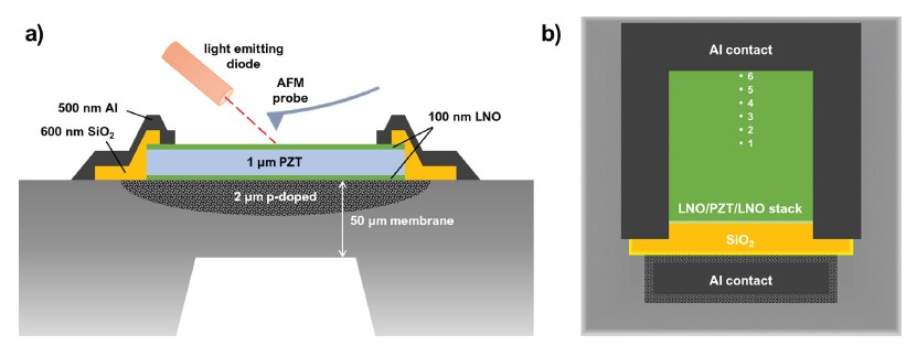
Figure 1. a) Sketch of the cross-section of the piezo-photomotion device. b) top view of the device; the numbering indicates the positions on the active area of the sample where measurements were performed.
The devices were placed into the NX10 microscope during the experiments. Illumination was provided by a light-emitting diode with a wavelength of about 630 nm which is a part of the PhotoCurrent Mapping (PCM) extension of the NX10 setup. The open design of the NX10’s AFM head provides large space above the measurement area and thus enables a lot of freedom in optimizing the angle of the impinging beam and its position on the active area of the device. Since the LNO/PZT/LNO stack is transparent in the spectral range of the diode, the light can reach the photodiode and hence generate a potential difference between the two electrodes, which leads to the deformation of the piezoelectric layer. Park Systems microscopes are designed as sample scanners, meaning that the probe always remains stationary in the center of the tool, while the sample mounted on a XY scanner can be displaced laterally. Since the light-emitting diode and the AFM head are fixed with respect to the sample stage, only one initial alignment is needed to have the emitted beam illuminating the probed area of the sample.
The light switching can be regulated via a triggering voltage. For that, an external function generator (GW Instek SFG-1003) was coupled with the triggering line of the emitter, leading to alternate light switching on/off periods with a pre-determined frequency. The rising time of the emitter, i.e. the time needed to reach the maximum power of the emitted light, is evaluated to be less than 1 μs.
Measurements were performed in KPFM mode, where the Contact Potential Difference (CPD) between the AFM probe and the sample is measured at each position during imaging. There are several ways to implement KPFM, all based on applying an oscillating electrical bias with a given amplitude and frequency between the tip and the sample. This electrical excitation creates peaks in the spectrum of the vertical deflection of the cantilever with an amplitude proportional to the CPD. Using a lock-in amplifier fed with this vertical deflection as an input signal, it is possible to evaluate the amplitude at given frequencies and apply an additional potential that counteracts the CPD and thus nullifies the total potential difference between the tip and the probe. In consequence, the deconvoluted amplitude is reduced to zero. For an extended discussion of KPFM, please refer to [3]. In Sideband™ KPFM, the frequency of the exciting bias is selected in such a way to produce peaks on the sidebands of the mechanical resonance of the probe. As a result, peaks in that range are enhanced. Moreover, the amplitude of these sidebands depends more on the contribution of the tip-sample interaction than on forces acting on other parts of the cantilever [4], leading to a better quantitative and laterally resolved determination of the potential.
KPFM can only be performed while scanning the sample in Non-Contact mode. Therefore, the system must be capable of deconvoluting both the amplitude of the resonant peak modulated by the sample topography, and the amplitude of electrically induced peaks modulated by the surface potential. The default Park Systems NX electronics are equipped with four independent lock-in amplifiers that can be run in parallel, plus a feedback servo acting on the tip DC bias. This allows for mapping the topography and potential simultaneously, with no need for a second pass at any scanned line in lift mode, and with greater accuracy due to the closer distance of the tip to the sample. The built-in EFM/KPFM environment in the Park Systems SmartScan™ software allows implementation of the Sideband™ KPFM mode in an effective and intuitive way.
Results
The active area of the fabricated devices is roughly a square with sides measuring a few millimetres. As a first test, the AFM probe was landed at the center of the membrane, in the position marked as 1 in Figure 1 b). Since the main focus of this test was Figure 1. a) Sketch of the cross-section of the piezo-photomotion device. b) top view of the device; the numbering indicates the positions on the active area of the sample where measurements were performed. Figure 2. a) Comparison of the displacement and photo-induced voltage versus time, with a light pulsed at a switching frequency equal to 1 Hz. The device behaviours in time at frequencies equal to 2 and 4 Hz are shown in b) and c) respectively. to determine the time dependence of the membrane response, the scanned area was reduced to a single point of zero lateral dimension in order to limit topographic crosstalk, and signals were acquired vs. time. Since an amplitude modulation-based feedback on the tip-sample distance was active during Sideband KPFM experiments, any vertical change of the surface position induced by the movement of the membrane could have been tracked in parallel to the potential shift. Here we will define as displacement the shift of the surface height with respect to its resting position.
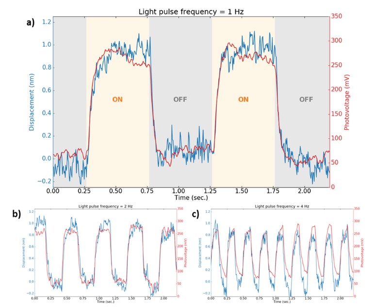
Figure 2. a) Comparison of the displacement and photo-induced voltage versus time, with a light pulsed at a switching frequency equal to 1 Hz. The device behaviours in time at frequencies equal to 2 and 4 Hz are shown in b) and c) respectively.
Figure 2 a) shows results when applying the light excitation with a frequency of 1 Hz (0.5 seconds on, 0.5 seconds off). The periods where light was switched on are indicated with a light orange background, while the dark periods are indicated with a light grey background. It can be noticed that whenever the light was on, a vertical displacement of roughly 1 nm upwards could be observed. In the same conditions, an increase in the surface potential of about 200 mV (defined as the difference between the top and bottom plateaux) was measured. This demonstrates the basic principle of the device: the voltage generated by the photodiode via illumination is applied to the bottom electrode resulting in the expansion of the piezoelectric stack. The 50 mV surface potential measured during the dark periods is due to the contact potential difference between the probe and non-excited sample.
More tests were performed at higher pulse frequencies and results for 2 and 4 Hz are shown in Figures 2 b) and c) respectively. A similar trend can be observed, with the total amount of displacement and photovoltage being sensibly smaller at 4 Hz. Also, it can be noticed that the plateaux become smaller at higher frequencies, while the presence of a transient time to reach the new status after light switching becomes more apparent.
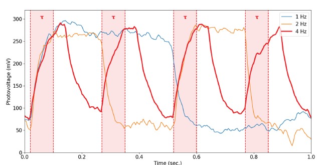
Figure 3. Photovoltage vs. time for light pulse frequency of 1, 2, and 4 Hz. The rising time of the photovoltage measured at 4 Hz is represented with a red background.
To better investigate the transient response time, photovoltage vs. time measurements were plotted together in Figure 3. The photovoltage measured with a pulse frequency of 4 Hz is represented in red with a total time range of 1 second. For each pulse cycle, the rising time τ spanning from the moment where the light has been switched on to the moment when the plateau has been reached is represented with a red background. The rising time has been estimated to be about 80 msec., which is much higher than the response time of the emitting diode indicating that τ is a characteristic response feature of the device. It is worth noticing that although the photovoltage appears reaching a plateau for all the data plotted, the difference between the two levels when applying 4 Hz pulse frequency appears slightly smaller than the other data. It is currently unclear whether this effect is due to the continuous excitation of the photoresponse at higher frequencies or to other experimental reasons. Before further analysis would clarify this point, we will assume the value of 80 msec. well representing the qualitative behaviour of the response as the correct rising time. Photovoltage at pulse frequencies equal to 1 and 2 Hz were also plotted. These signals were conveniently shifted on the x-axis to have the light pulse start at the same time. Here, τ is in good agreement among all the measurements. A model to describe the time response of the device is currently under development by IMS, although it has been hypothesized that it may be linked to the quality of the interface between the photodiode and the bottom electrode. The here presented experiments provide crucial information about the expected performance of the device at different communication rates with respect to the exciting light source and about the efficiency in converting the transmitted signal into a movement.
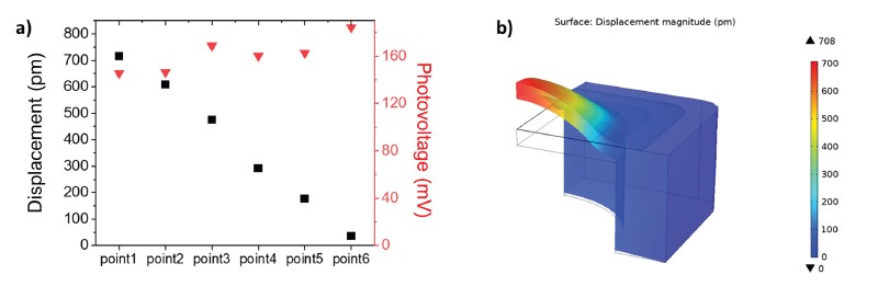
Figure 4. a) Mechanical displacement and surface potential at the positions indicated in Figure 1. b) 3D rendering of one quarter of the device representing the vertical displacement of the PZT membrane.
On a similar device, the AFM probe was approached in six different positions progressively farther distanced from the center and numbered as in Figure 1 b), with the goal of measuring the membrane vertical displacement and light-induced photovoltage as a function of the position on the membrane. Light pulses with a frequency of 8 Hz were generated to excite the membrane. The results of this experiment are shown in Figure 4 a). It can be seen that the displacement and photovoltage vs. position have different trends. In the case of the displacement, the maximum value is observed at the center of the membrane, while there is a decrease to almost zero displacement when reaching the side of the membrane. The displacement at the center is about 700 pm and then smaller than what reported for the other device, which can be due either to small structural variations among different devices, or to the fact that when using an 8 Hz frequency the light on/off time is 62.5 msec , which is slightly lower than the estimated 80 msec. rising time. Therefore, the higher pulse frequency may prevent the membrane from reach the displacement plateau.
On the other hand, the photovoltage remained more or less constant at the different positions. This consistency may be simply due to the homogeneity of the silicon layer at the bottom of the device, providing the same photo-response everywhere. Again, additional simulations could shed further light on the underlying mechanisms to support any interpretation of these observations. A hypothesis for the decreasing amplitude of the displacement with increasing distance to the center could be found in a mechanical restriction since the membrane is attached at its borders to the support of the sample, resulting in a smaller free oscillation.
Conclusion
In this application note, we have demonstrated the working principle of piezo-photomotion devices. We have shown how AFM and in particular the setup and options offered by the Park Systems NX10 AFM is the suitable choice to explore the properties of such devices. KPFM measurements of the light-induced displacement and photovoltage as a function of time and of the position along the device membrane have been discussed. We reported the expected time response of the membrane expansion and voltage change. We showed the presence of a rising time from the switch-off to switch-on status allowing us to estimate the highest rate at which the membrane can react to external light excitation at full efficiency. Finally, we commented on the dependence of the displacement on the position along the membrane linking it to the mechanical constraints given by the geometry of the device, and on the homogeneity of the photovoltage response. The ensemble of these measurements enables the investigation and optimization of piezo-photomotion and other types of light-driven devices.
References
[1] W. M. Luiten, V. M. Van Der Werf, N. Raza, and R. Saive, “Investigation of the dynamic properties of on-chip coupled piezo/photodiodes by time-resolved atomic force and Kelvin probe microscopy,” AIP Adv., vol. 10, no. 10, Oct. 2020, DOI: 10.1063/5.0028481.
[2] Z. Zhan, F. Wei, J. Zheng, W. Yang, J. Luo, and L. Yao, “Recent advances of light-driven micro/nanomotors: Toward powerful thrust and precise control,” Nanotechnol. Rev., vol. 7, no. 6, pp. 555–581, 2018, DOI: 10.1515/ntrev-2018-0106.
[3] A. Axt, I. M. Hermes, V. W. Bergmann, N. Tausendpfund, and S. A. L. Weber, “Know your full potential: Quantitative Kelvin probe force microscopy on nanoscale electrical devices”, Beilstein J. Nanotechnol., vol. 9, 1809–1819, 2018, DOI: https://doi.org/10.3762/bjnano.9.172
[4] J. Colchero, A. Gil, and A. M. Baro, “Resolution enhancement and improved data interpretation in electrostatic force microscopy”, Phys. Rev. B, vol. 64, 245403, 2001, DOI: 10.1103/PhysRevB.64.245403